Source: www.analog.com
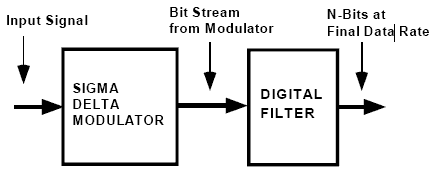
Sigma delta conversion is a technique that has gained popularity for high-resolution applications. The main components of a sigma delta converter are a sigma delta modulator and a digital filter as shown in Figure 1.

Figure 1. Sigma Delta ADC
The sigma delta modulator samples the analog input at many times the Nyquist rate and produces a 1-bit output whose average value tracks the analog input. This one bit data stream is processed by a digital filter to produce a high resolution conversion result. A model for a typical first order sigma-delta modulator is illustrated in Figure 2.

Figure 2. First Order Sigma-Delta Modulator
The analog modulator consists of a sampling capacitor and a 1-bit A/D converter in an analog negative feedback loop with high open loop gain. The feedback works to minimize the error between the input signal and the feedback signal. This procedure is essentially a digital process and the linearity performance is determined by the sampling capacitor. With the circuit shown in figure 2, the analog input signal and a bit-stream whose 1's bit density is a representation of the magnitude of the analog signal are fed into a summing amplifier. This is then integrated and enters a comparator that outputs a 0 or 1 depending on whether the output of the integrator is below or above the comparator's threshold. The average density of the bit-stream closely tracks the analog input signal. Any deviation will quickly result in the average bit-stream density from the comparator being adjusted to follow the analog input signal. This action forms a high gain, negative feedback loop which gives the sigma-delta ADC excellent linearity and no missing codes. It also minimizes the effects of component drift with time making the sigma-delta very stable compared with other architectures. The modulator over-samples the input and spreads the quantization noise from DC up to a bandwidth of fs/2. Thus the noise density in the band of interest is much reduced. In general, over-sampling alone is not enough to achieve the required resolution. Noise shaping achieved using spectrum where it can be removed by the digital filter. Therefore to achieve the high resolution in a sigma delta converter, a combination of three techniques are used; over-sampling, noise shaping and digital filtering.
What architecture is used?
This family of ADCs use a sigma delta architecture consisting of a second order modulator followed by a third order sinc^3 filter. This combination of second order modulator and third order filter offer many advantages over the first order modulator described earlier. The use of a second order modulator gives better noise shaping -more noise is pushed outside the band of interest that leads to better resolution. A second order modulator gives a 15dB increase in resolution for every doubling of the sampling rate compared to 9dB for a single order system. This allows high resolutions to be achieved with lower sampling rates. Lower sampling rates ease the requirements on the system clock and also reduce the power requirement, allowing low power designs to be implemented. The modulator's sampling rate on this family is 19.2kHz when operated with the standard 2.4576MHz clock.
The filter used on these parts is a sinc^3 digital filter. The response of this filter is similar to that of an averaging filter but has a sharper roll-off. Sinc^3 filters provide linear phase response and the -3dB frequency is located at (0.262 * the first notch frequency). The output rate of the digital filter corresponds to the positioning of the first notch. Further notches of this filter are placed at multiples of the first notch. Therefore if the first notch is placed at 10Hz, then the filter will provide rejection in excess of 100dB at both 50 and 60Hz. The settling time associated with this filter is directly related to the output data rate. The settling time of the digital filter is four times the update rate for a step change on the analog input. When switching between channels, the settling time is three times the programmed update rate.
How is the programmable gain function implemented?
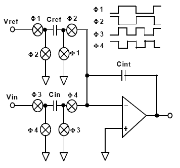
Programmable gain is implemented using a combination of multiple input sampling per modulator cycle and scaling of the ratio of reference capacitor to input capacitor. Programmable gain is implemented using switched capacitor techniques. This is achieved by altering the sample rate of the input capacitor in the analog modulator. This technique is shown in figure 3.

Figure 3. Programmable Gain Implementation
In this circuit, the reference capacitor Cref is used to sample the reference voltage Vref using non-overlapping clocks ?1 and ?2 at the modulator sampling frequency fmod. The input capacitor Cin samples the analog input voltage again using non-overlapping clocks ?3 and ?4 with a sampling frequency of fin. If fmod is equal to fin, the implemented gain is equal to the ratio of Cin to Cref. With the timing shown in figure 3, fin = 2fmod, thereby implementing a gain of 2 when Cin = Cref.
What are the advantages and disadvantages of sigma-delta ADCs?
The penalty paid for the high resolution achievable with sigma-delta technology has always been speed: the hardware has to operate at the over-sampled rate, much larger than the maximum signal bandwidth, thus demanding great complexity of the digital circuitry. Because of this limitation, ??? converters have traditionally been relegated to high-resolution, very-low frequency applications and more recently speech, audio and medium speeds (100 kHz to 1 MHz).
The digital filtering stage results in long latency between the start of the sampling cycle, and the first valid digital output; similarly, there is a significant lag thereafter between digital outputs and their corresponding sampling instants. These characteristics reduce the throughput time in multiplexed systems as it takes many clock cycles for the digital filter to settle after switching from one channel to the next.
Most of the circuitry in sigma-delta converters is digital, allowing these converters to be fabricated on a wide range of IC processes. This implies that performance will not drift significantly with time and temperature. They are inherently monotonic (i.e., a change in the digital output has always the same slope as the analog input). This is of particular importance in closed-loop control systems, where misinterpretation of the direction of change of a measured variable may cause the system to become unstable. They are inherently linear, and present little differential non-linearity. External sample & hold circuits are not required due to the high input sampling rate and low precision of the A to D conversion within the modulator, (the devices are inherently self-sampling and tracking). Requirements for analog anti-aliasing filters are minimum - in most cases, a simple single pole RC-filter suffices as the bandwidth of interest is considerably lower than the first image which occurs about the modulator frequency. In contrast, the filters required for medium- to high-resolution applications using other (non-oversampling) technologies are very sophisticated, difficult to design, large, and expensive.
What was the traditional approach to analog front end solutions and how do sigma delta solutions overcome their shortcomings?
Traditional approaches to the problem of measuring signals from transducers have been to use a high resolution Analog to Digital Converter (ADC) as the core element in the process. These were generally integrating ADCs or voltage to frequency converters (VFC) that provided high resolution for low input bandwidth signals. This ADC had to be surrounded by a considerable amount of analog signal conditioning circuitry to boost the transducer output signal so that the full dynamic range of these converters could be used to achieve the required performance. The performance of this signal conditioning circuitry, rather than the high-resolution converter, often determined the system success in measuring low-level signals. In designing gain stages, a number of factors have to be taken into account; the first and most critical is noise, both in the measurement environment and in the components that constitute the high gain stage. Common sources of noise in the circuit design environment are mains frequency noise and power supply noise. Other causes for concern include common mode rejection of the gain stage as the transducer output may sit on a large DC signal, therefore necessitating conversion from a differential input signal to a single ended output. Offset in the amplifiers along with drift performance play havoc with circuit performance, leading to the use of expensive chopper stabilized amplifiers. Programmability was difficult to design into these systems and calibration was performed mainly with the use of the system micro-controller. This leads to the requirement for external memory to store calibration coefficients.
Recent advances in design techniques incorporating switched capacitor and sigma delta technologies have enabled low cost, low power, highly accurate and integrated solutions to be developed. These architectures address the real-world problem of low-power design required for data acquisition applications. The advantages that an integrated solution offers the system designer include signal conditioning necessary for direct transducer interface integrated on chip that greatly reduces analog circuit design and layout complexity. Integrated solutions also offer better control of specifications and error budgets than those of discrete solutions. Sigma delta converters provide enough dynamic range to allow direct transducer interface, thus removing the need for a high gain signal conditioning stage in front of the ADC.
In any application, what determines the most suitable ADC?
In selecting an ADC for any application, there are a number of key selection parameters. These include required resolution, number of input channels, supply voltage and power consumption, analog input range, interface and achievable performance. The sigma delta selector guide at www.analog.com gives the complete list of low bandwidth, high resolution ADCs available from Analog Devices. The selector guide highlights the key features of each ADC along with identifying the most suitable ADCs for several industrial applications.