Acta Electrotechnica et Informatica No. 3, Vol. 6, 2006 1
Jaroslav DUDRIK Department of Electrical, Mechatronic and Industrial Engineering, Faculty of Electrical Engineering and Informatics, Technical University of Kosice, Letna 9, 042 00 Kosice, Slovak Republic, tel.: +421 55 602 2276, E-mail: jaroslav.dudrik@tuke.sk
Soft-switching DC-DC converter using Phase-Shifted Pulse Width Modulation (PS-PWM) on secondary side of highfrequency transformer is described in the paper. The converter consists of a full-bridge inverter fitted with fast IGBT transistors. The output power of the converter is controlled by rectifier made up of two snap-off diodes in series with MOSFET transistors which is connected on secondary side of high-frequency power transformer. This topology can easily achieve soft-switching operation also under low commutating current. The conduction losses are substantially reduced compared with conventional soft-switching DC/DC converters. The converter has been designed for arc welding with output power of 1.5 kW and switching frequency of 50 kHz.
Keywords: DC power supplies, soft switching, ZCS converter, ZVS converter
Along with increasing demand for high power density conversion the IGBT transistors are preferred to MOSFETs in high power range applications. IGBT transistors are designed for higher rated voltages and currents and they have lower conduction losses compared MOSFETs. However, the IGBTs are slower than MOSFETs (IGBT frequency is usually limited to 20 - 30 kHz) because of higher switching losses which come from the tail current at turn-off. Hence, if the IGBT transistor is to be utilized for higher switching frequencies the turn-off losses should be minimized. A solution may be either zero voltage switching (ZVS), which is effected by adding an external snubber capacitor or zero current switching (ZCS). Zero current switching seems to be more efficient that zero voltage switching since the tail current problem can be eliminated to a minimum by removing the minority carriers before turning off [1], [2].
The soft-switching techniques applied to the power converters have attracted attention for its peculiar advantages over the hard-switching techniques such as low switching loss, high-power density, EMI/RFI noise reduction and so on [5], [6], [7], [8].
Most of full-bridge DC/DC converters are controlled by Phase-Shifted PWM scheme. However the soft-switching PS-PWM DC-DC converters have some difficulties to be solved. The conduction losses of conventional soft-switched converter are relatively high due to the circulating current flowing through the primary winding of the high-frequency transformer during freewheeling period. The converter needs a large commutating current in order to ensure ZVS operation. The proposed DC-DC converter can nicely solve these problems mentioned above. As a result, the conduction losses caused by circulating currents are substantially reduced compared to those produced by conventional softswitching PS-PWM DC-DC converters.
The conventional basic DC-DC converter operates with PS-PWM control at constant switching frequency. Value of the output current is controlled by change of the phase shift between the leading (transistors VT1, VT4) and lagging leg (transistors VT2, VT3), respectively.
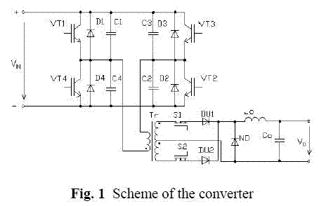
On the contrary to classic solution pulse width modulation with phase shift on secondary side of high-frequency transformer is used in the proposed PS-PWM DC-DC converter. The full-bridge inverter VT1 - VT4 is controlled with constant switching frequency and with no phase shift between leading and lagging leg of the inverter. So the inverter only operates with 50% duty cycle and thus cannot influence the output voltage value. Switches S1, S2 in series with the output rectifier diodes DU1, DU2 are added to secondary winding of the power transformer. The scheme is shown in Fig. 1.
Value of the output voltage or current is controlled via the phase shift between the inverter switchesVT1-VT4 and switches S1, S2 on secondary side of high-frequency power transformer Tr. The waveforms of the DC-DC converter with secondary switches are shown in Fig. 2.
The operation principle of the proposed DC/DC converter is described as follows.
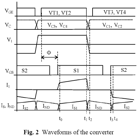
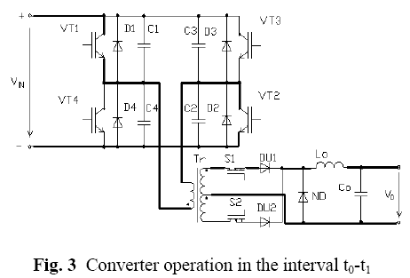
TIn this interval the primary current flow through inverter switches VT1, VT2, secondary current through switch S1 and diode DU1. The energy is transmitted from input to output of the converter until the inverter transistors VT1 and VT2 are turned-off at time t1.
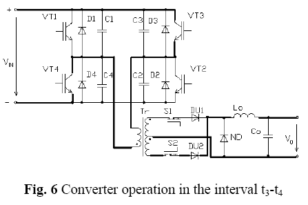
When the inverter switches VT1, VT2 are turned-off at time t1, the commutation current charges the capacities C1, C2 to DC input voltage value VIN. The rate of rise of the collector voltages of VT1, VT2 is slowed down by snubber capacitors C1, C2 and thus the reduction of turn off losses is ensured. The primary voltage V1 changes its polarity. The diode DU1 is turned-off when primary voltage V1 changes polarity from positive to negative. At the end of this interval the capacitors C1 a C2 are fully charged to input voltage VIN and the capacitors C3 a C4 are discharged to zero voltage and therefore the diodes D3, D4 start conducting. The secondary switches S1, S2 are turned off under ZCS and output current starts to flow through freewheeling diode ND.


Operation of the proposed converter was verified on laboratory prototype. The result was measured at input voltage VIN=300V. The maximum output power of the converter was 2.5 kW at switching frequency of 50 kHz.
The following components were used in the power stage:
T1-T4 - IRG4PC50W, ultra-fast IGBT transistors D1-D4 - HFA25PB60 , freewheeling diodes DU1, DU2 - BYW 255V, output rectifier S1, S2 - IRFP260 (two in parallel), output rectifier Power transformer: Lm = 2.85 mH, magnetizing inductance, LL = 3.4 µH, primary leakage inductance, n = 6, transformer turns ratio Smoothing inductance: L0 = 12 µH Turn-off snubber: C1 - C4 = 3.9 nF, snubber capacitancesSpecial PS-PWM controller UCC 3895 is implemented for the converter current mode control. It is easy to assemble an integrated gate driver UC3708 with isolation transformer because duty ratio for transistors is almost 50%.
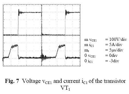
The switch voltage vCE1 and switch current iC1 of the transistor VT1 in the inverter is shown in Fig. 7. The transistor is turned-on under zero-voltage switching. Because of symmetry of the leg the transistor VT4 works under the same operating conditions.
The turn-off loss is reduced by capacitors C1, C4 acting as the nondissipative snubbers.
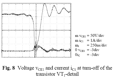
The detail of the turn-off transition is shown in Fig. 8. It can be seen that the turn-off losses are considerably reduced. The only tail current of the transistor causes some turn-off losses.
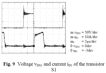
Fig. 9 shows the voltage and current of secondary side MOSFET transistor S1. The turn-on and turn-off is under ZCS.
The properties of the converter were verified at the arc welding application, where the full range of the load current from no-load to short circuit occurs.
Fig. 10 shows the dynamic properties at transition from short circuit to no-load of the converter. At short circuit a slightly higher load current appears as a result of delay time of the control pulses.

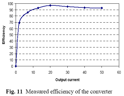
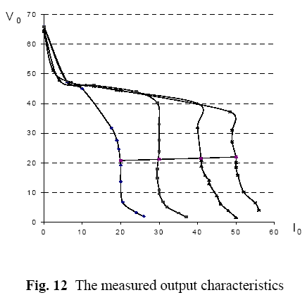
The efficiency of the converter is illustrated in Fig. 11. At nominal output power the efficiency is over 90%. The measured output characteristics of the welder including added arc characteristic are shown in Fig. 12. The output no-load voltage is about 65V, which is enough for arc burning at normal operating conditions. In the working area the converter behaves as an adjustable current source keeping the set welding current value.
[1] Kozurou Harada: Analysis and Design of ZVSPWM Half-Bridge Converter, IEEE PESC Record, 1995, pp. 280-285.
[2] Masakazu Michihira: A novel quasi-resonant DC-DC converter using phase-shift modulation in secondary side of high-frequency transformer, IEEE PESC record, 1996 pp. 670- 675.
[3] M. Horvбth, J. Borka: Welding Technology and Up-to-date Energy Converters, EDPE 2005 Conference, Dubrovnik, Croatia, September 24-26, 2005. CD-Proc. E05-06.
[4] J. Dudrik: Current Source for Arc Welding, Elektro (journal), 1993, No.1, pp. 450-455 (in Slovak)
[5] I. Feтo, E. Jadroт, P. Њpбnik, Using Partial Series Resonant Converter in Heavy Duty Welder, In Conf. Proc. ELEKTRO 2001, section - Electrical Engineering. Ћilina 2001, pp.76 – 81.
[6] P. Bauer, K. Bauer: Modern Power Electronics, ISBN 909010243-4, 1996.
[7] J. B. Klaasssens, M. P. N. van Wesenbeeck, P. Bauer: Soft Switching Power Conversion; European Power Electronic Journal, Brussels, Sept.1993, Vol. 3, No. 3, pp.155-166.
[8] J. Dudrik: Soft Switching PWM DC-DC Converters for High Power Applications , Proc.of the Int. Conf. IC-SPETO 2003, Gliwice-Niedzica, Polen, 2003, pp.11-11a-11f- 12.
[9] P. Chlebiљ, J. Hrabal: Possibilities of power losses reduction in semiconductor converters In: DRIVEґ97, Ostrava, Czech Republic, 1997, pp. 83-88, (in Czech)
[10] Z.Sьtх, I. Nagy: Study of Nonlinear Dynamics of Current Controlled Converter Embedded in a General Approach of Variable Structure Systems, In:10th European Conference on Power Electronics and Applications, EPE’2003, 2-4 September, 2003, Toulouse, France. CD Rom ISBN:90-75815-07-7
Jaroslav Dudrik received the M.S. and Ph.D. degrees in electrical engineering from the Technical University of Koљice, Slovakia, in 1976 and 1987. He is currently associate professor of Electrical Engineering at the Department of Electrical, Mechatronic and Industrial Engineering, Technical University of Koљice, where he is engaged in teaching and research. His primary interest is power electronics. His field of research includes dc-to-dc converters, high power soft switching converters, converters for renewable energy sources and control theory of converters.
This work was supported by Scientific Grant Agency of the Slovak Republic under contract VEGA No. 1/2178/05.
ISSN 1335-8243 © 2006 Faculty of Electrical Engineering and Informatics, Technical University of Koљice, Slovak Republic
| ДонНТУ | Автобиография | | Реферат | | Ссылки | | Отчет о поиске | |
| Портал магистров ДонНТУ |