DESIGN AND DEVELOPMENT OF LOW NOISE AMPLIFIER USING 3-DB QUADRATURE HYBRIDSVandana K. Ramchandra
Source of information: http://www.rfcafe.com/references/articles/LNA-Design-Using-Quadrature-Hybrid.pdf |
||||||||||||||||||||
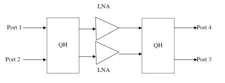
AbstractThis paper describes and discusses a procedure of how to design RF/Microwave Low noise amplifier with minimum noise figure and low VSWR. The initial data available is S-parameters of the device. This paper references the RF design tool called ADS by Agilent technology. I have tried my level best to provide the methodology to reduce the noise figure and return loss in the same circuit without using the isolator which is the well known trade-off in the design of LNA. This method also reduces the cost of the amplifier when compare to other amplifiers which uses isolator for good VSWR. I am thankful for the blessings of God. I dedicate this paper to my parents, sisters and friends who had encouraged me. IntroductionThe low noise amplifier is used as the front end amplifier of Receiver so that the receiver sensitivity is improved by low noise figure and high gain in the first stage. Usually there is a trade-off between the two important parameters of LNA namely noise figure and VSWR in the design of LNA but this paper gives the path to remove the trade off and presents good VSWR along with low noise figure. Generally to attain good VSWR in LNA, isolators with low loss are used at its input which increases the cost of the amplifier but this paper illustrates a brilliant explanation of the design of LNA in which QH is used in order to attain good VSWR and it also decreases the cost of the amplifier. These QHs are cascaded with amplifiers as shown in the block diagram below. This paper presents the complete design flow of Low noise amplifier (LNA) starting from the selection of device to the testing of amplifier. This introduction section gives the block diagram and its description in detail.
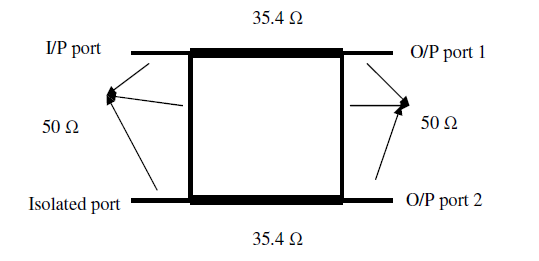
Description of the block diagram: It is a four port device in which two amplifiers are cascaded parallel to each other. Port 1 is the input port through which input is fed to the amplifier. Port 2 and port 4 are terminated by 50 Ohms since they are isolated ports. Port 3 is the output port. In between the two 3-dB Quadrature hybrids, two low noise amplifiers which are perfectly designed for lower noise figures are connected. These low noise amplifiers have NF of 0.2 dB and VSWR of 2:1. but by cascading them with the QH their VSWR appears to be 1.2:1. this is the technique in this paper. DESIGN PROCEDURE AND EXAMPLE:The EDA software used is Agilent Technology manufactured ADS. Before choosing the substrate on which the LNA has to be designed, the amplifier is designed taking ideal conditions (o dB substrate loss with dielectric constant of 1) in to considerations once it is fully designed then the substrate is introduced which hinders a little of its performance. The design is carried out in the following way: Design procedure: a) Quadrature hybrid is designed by the transmission lines which have the 35.4 and 50 Ohms impedances. It is as described by the following figure:
b) The device for LNA is selected which suits the required frequency range. c) The input reflection coefficient (S11) of the selected device is placed in the simulation environment then it is slowly matched to 50 Ohms by adding distributed elements and lumped elements at the input of the device. Care should be taken for input lead width of the device and the transmission line at the input of the device. d) Similarly output reflection coefficient is matched to 50 Ohms of the system. e) Most care is taken when placing the biasing elements so that the performance is not hindered by adding the biasing inductors and capacitors. f) While selecting the substrate the power handling of the amplifier is the most important consideration. g) After selecting the substrate and introducing it in the design little tuning and optimization is required to meet the performance. h) ADS design tool has a feature of generating the layout automatically. i) Once the layout is finalized then it is sent for PCB fabrication. j) As the PCB get fabricated final QC has to be made on it so as to avoid any mistakes. k) Then amplifier is assembled which is the replica of the design. l) Once it is assembled, PCB is packaged, connectorised and then it is tested for the specification laid.
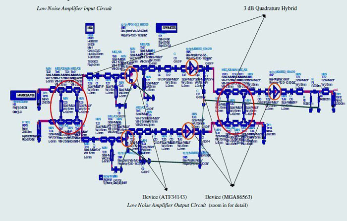
Example: Here I am presenting one example of LNA design using ADS with the specifications. This is the typical example of LNA which is used as the front end of the receiver. This receiver, along with the transmitter is used as a transceiver for an unmanned aerial vehicle which covers a range of more than 5 Km. The procedure follows as below: a) Specifications: LNA requirements are Frequency range: 2.4-2.5 GHz Gain: 56 ± 1 dB IF input Power: -98 dBm (nom) NF: 0.5 dB I/P VSWR: 1.5:1 O/P VSWR: 1.5 Mechanical size: 2”X2”X1” (along with the package) Connectors: SMA (f) b) Circuit diagrams:
c) i) Input circuit description: As there is a design trade off between VSWR and NF in LNA, 3-dB Quadrature hybrid is used at the input and output to reduce VSWR of the amplifier. 3-dB Quadrature hybrid is a four port network in which port1 is input port, port2 is isolation port, port3 and port4 are two o/p ports which divide the i/p power to half each and two o/ps being 90° out of phase. When these two Quadrature hybrids are combined together with the two o/p back to back then it will be perfectly matched to 50 Ohms and with min loss. This is a two stage Low noise amplifier to reduce the noise figure. The stage $between the two Quadrature hybrids is considered as one stage. The devices used are ATF34143 and MGA86563. The device used in the second stage is MGA86563 and it is used to provide the required gain. Input, output and interstage matching is done using distributed elements such as microstrip lines and lumped elements. DC coupling and DC biasing capacitors are placed carefully so that the amplifier performance is not disturbed. Choke inductor is placed at the biasing points so that better isolation is provided between the DC and RF paths. The input power fed to this amplifier is -98 dBm. ii) Output circuit description: As observed in the o/p file both input and output impedances are matched to 50 ohms. The NF of the amplifier is 0.3 dB (nom) and the gain of the amplifier is 56 dB Hence the output power from this amplifier will be -41 dBm. PRACTICAL PERFORMANCE AND SUGGESTIONS:Practical performance: As expected the practical performance will not meet the designed results. The following table gives the comparison between the theoretical and practical results: Comparison table
Suggestions The following are the suggestions for improving the performance of LNA: a) While generating the layout care should be taken for undercuts and apart from the designed transmission line length, some extra length should be added for assembling the lumped elements so that its original length doesn’t get disturbed. b) Care should be taken in using the lead while assembling the devices or lumped elements. c) Biasing points should be given highest priority since the devices used are d) The PCB should be perfectly packaged in an aluminium package so that there should not be any air gap between the centre pin of connector and the transmission line on which it is to be soldered. e) After supplying the DC voltage, it is checked for stability on Spectrum analyzer. If there are no oscillations then the amplifier is perfectly stable else it should be stabilized by tuning the circuit with different values of capacitor between the transmission line and ground made it stable. f) Once the amplifier is stabilized then it is tested for gain, VSWR using network analyzer and NF using Noise source, preamplifier and spectrum analyzer noise measurements. g) The amplifier is tested for output power using signal generator to feed RF power and spectrum analyzer to see the output spectrum. SUMMARYLow noise amplifier is designed for low NF, high gain, good VSWR using design tool ADS, manufactured by Agilent technologies. The main objective of this paper is to present a methodology for low NF and good VSWR using Quadrature hybrid. By selecting proper devices the LNA can be designed using ADS and the Quadrature hybrid is designed using impedance matching technique. After designing the LNA using the techniques described in previous sections, it is fabricated on the selected substrate and tested for the performance. Practical results were compared with the theoretical ones and tabulated. Some suggestions were also listed which facilitates the engineer to approach the theoretical results after fabricating with minimum distortion in performance.
|