

Navigation
Changeover to digital methods of transfer and commutation, except for advantages conditioned by new communication technologies,
aroused many problems specifically connected with principles of signaling in digital form, and one them is a problem of synchronization.
Among those parameters characterizing synchronization signal one can distinguish jitter (phase jitter) as caused by change of signal
delay time in connector circuit between components. Jitter is always available in digital communication systems, but with a certain
value being exceeded jitter starts to affect the quality of information transfer. A new technique is proposed to record influence of metering circuit capacity self-discharge on jitter measurement accuracy.
Measuring procedure was improved. The goal of this work is extension of application field for jitter measurements into practice of adjustment and operation of
digital telecommunication channels at the expense of improvement of measurement instruments techniques.
Introduction and motivation
With sequential information flow reception it is an ideal case, if information readout is made in the middle of timing bit slot.
Availability of jitter influences decision making as regards to the bit being received in the decision device. In case of multiple
regeneration of digital flow jitter usually increases, which may cause either bit errors rise (BER) or total system failure because of
synchronization system fail. Possible causes are:
• incidental phase modulation in bit-timing frequency generators;
• noise and interference impact on synchronizing circuit in the receiver
• transmission path length change
• propagation speed change;
• Doppler shift from moving objects
• irregular timing information entry etc.
The is why engineering design of a device for jitter measurement and depletion is so much actual for development of communication
systems with several regeneration (rebroadcast) and multihop wireless communication systems.
Scientific novelty
The bottom line of this work being planned is to make digital simulation of measurement units realizing the technique in accordance
with the designed structure.Goals and objectives
It is necessary to solve the following main objectives to reach the target goal:
Review of researches in this sphere
On the university level
Developments concerning this and other topics connected with jitter measurement by means of PLL in Donetsk National Technical
University are carried out under the guidance of Professor Aleksandr Grigorjevich Vorontsov.
Search on the site of DonNTU masters shows three Master's Theses on topic:
1. "Research and development of technical facilities of laboratory research for study of PLL systems’ characteristics and properties in
the electric coupling theory course" of Rakitina Anastasiya Yuryevna
2. "Research and development of signal spectral estimation techniques for solution of telecommunication systems’ objectives" of
Khmelevoy Oleg Vladimirovich.
3. “Research of interconnect in cable lines as reasons for jitter rise in digital communication systems” of Libatskaya Olga Nikolayevna.
On the national level
Рas of today solution of problems connected with jitter measurement in Ukraine unfortunately is not available. This subject matter has been actively studied in USSR periods. For example, this matter is considered in the book of A. P. Gorshkov “Apparatus for frequency and time variations” [3].
On the world level
Here it is possible to refer to a set of documents and articles dedicated to jitter measurement in telecommunication systems. This direction is being intensively studied in the USA and China. The example is a Mater’s Thesis of a student from Taiwan University Tsan-Huei Wu [6], dedicated to the issue of jitter measurement in PLL system.
Main part
Analysis of object of research
In the process of signal transfer from the source to the receiver the signal is always subject to distortion. Distortion
appears at the account of the signal being affected by the most variable noises (transferable bit). Noise is defined as any
undesirable electric energy that appears within the limits of communication channel free transmission range. Ideal digital
signal can be presented in the form of trapezium with the final rise time (from 0 to 1) and decay time (from 1 to 0). With
interferences being available the signal is introduced as a sum of ideal signal and noise, with the signal loosing its ideal
form as shown in the Figure 1.

Figure 1. Noise effect on the signal
(animation: volume - 10 KB; size - 450х199; delay between the last and first shots - 1000 ms; number of repetion cycles - continuously)
(animation: volume - 10 KB; size - 450х199; delay between the last and first shots - 1000 ms; number of repetion cycles - continuously)
As can be seen the signal is distorted in two aspects: phase and amplitude signal deviation. Amplitude signal distortion is called amplitude distortion (or just noise), and phase signal deviation is called phase jitter (or just jitter).
Formal definition of phase jitters is given by ITU-T 0.171 – “Short-period deviations of digital signal meaningful positions from its ideal time position”.
Two main approaches to jitter definition are spread on practice - in phase terms and in frequency terms [1]. Both approaches are equivalent ones. The approach to description of jitter in terms of phase instability of the received digital signal is a spread theoretical process description. Spread of this approach caused emergence of jitter definitions as a phase jitter. However, for the purpose of practical measurement of jitter parameters its consideration within phase terms appeared to be inconvenient and it is connected with objective difficulties of phase measurements. It resulted in emergence of jitter applied consideration as a variation of received signal frequency. In this case the main jitter parameters become its amplitude and frequency. Such a consideration has got a wide practical application on measurement techniques and in the technique of results’ analysis. Naturally phase variations are connected with frequency variations by differential relations, so both considerations are equivalent in this sense.
At present time jitter value in the periodic signal is evaluated by three main ways [2]:
Period jitter–Jee. It is the most wide-spread technique of jitter measurement. The idea is the following: let clock pulse get over threshold level in Tee(n), where n is index of this period, and T0 is a lock pulse period, then jitter value can be mathematically described in the following way (Figure 2):
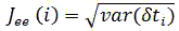

Figure 2. Period jitter–Jee
Cyclic jitter – JCC, is defined as a difference by time between two related cycles Figure 3. It does not contain information about degree of correlation between switching. This technique is an optimal one for measurement, when flicker noises are available in the system.
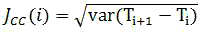

Figure 3. Cyclic jitter – Jcc
Long-term jitter or jitter of k cycles – Jk. Jitter Jk is a function from k and represents a general case of Jee jitter Figure 4. Mathematically it is described in the following way:
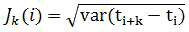

Figure 4. k Cyclic jitter - Jk
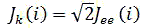
There is an interrelation between Jk(i) and Jee(i), which is defined by the following formula:
Practically all these three considered techniques of jitter measurement can be realized on oscillograph in the form of eye diagram. For this purpose a double-beam oscillograph is required, one input of which is supplied with a calibration signal, and the second one – with a test one. If oscillograph is clock cycled from the calibration signal and display is scaled to by time just in one period T, a set of pulses following each other will be displayed as a one, overlapping each other because of afterglow of screen luminophor dots. Such a specific Figure is called an eye diagram (Figure 5).

Figure 5. Eye diagram
Therefore one can see in the screen deviation of pulses from calibration signal, and it allows evaluating jitter of period Jee. With the same result cyclic Jcc and long-term Jk jitters are defined. It is just necessary to do scaling of display by time exactly for two 2T or several periods NT (N>>1), accordingly. Details of jitter measurement techniques we shall consider in the following chapter of the author's abstract.
Analytical review of existing methods and instruments for measurement of jitter in telecommunications
There are many ways of observation and measurement of the jitter affecting device, each of them is able to clear up its
origin. As we have already said the easiest and understandable by intuition way is jitter evaluation by eye diagram [3]. Eye
diagram type gives a lot of information about signal jitter as well as about many of its other parameters. For example, many
separate fronts and decays certify about possible jitter presence depending on data. Special test signal is not required for
eye diagram, though, if desirable, it is possible to use measuring signal of impulse generator. It can be successfully applied
while studying hash and disorganized data, and relates to range measurements.
Another way of jitter evaluation is histogram. Histogram represents the arrangement of value set given by the parameter being
measured (usually time or value marked on X axis) depending on frequency of their emerging (axis Y).
Histogram provides the level of understanding which is inaccessible for eye diagram. While searching for malfunction
characteristics of the signal as time of rise and decay, period and duty ratio can be displayed at histogram. These histograms
illustrate distribution of efficiency for different operation modes, which can be correlated with circuit functionality
conditions, for example, type of transferred sequence.
Key application of histograms is distribution of value frequency of Time Interval Error (TIE) for all bit junctions of the
signal measured. TIE is a difference in time between actual and prospective cross-points at eye diagram. Histogram of TIE
values is a main data set for procedures of jitter separation required by different standards of digital pipes.
In Figure 6 eye diagram and TIE histogram connected with it are shown. Eye diagram is shifted in such a way so that in the
center one could see a transition region (cross-point) between two “eyes”. Two separate lines of fronts and decays are traced
at the diagram, which certifies of availability of occasional jitter. Histogram of crosspoints on the eye diagram has two
maximums, and it distorts Gaussian curve. It points to the fact that the signal has both determinate and occasional components
of jitter.

Figure 6. Eye diagram and related TIE histogram
The above given ways of jitter observation at present time are mainly used in measurement systems for jitter laboratory analysis. In field measurements practice such a technique of jitter measurement did not find distribution as its realization in devices appeared to be very expensive.
The following way of jitter evaluation is in use of discrete calculation technique. (DCT) [4].
The essence of DCT is in the fact that the jitter, the amplitude of which is to be measured, is charged with lock pulses, the frequency whereof should at least be by an order higher than the signal being measured. If this number of lock pulses is counted, jitter size can be easily measured.
Block scheme of he proposed jitter measuring set is given in the Figure 8. There are two forming devices FD1 and FD2, a control device Cd, two time selectors ВС, a count pulse generator CPG, and a data analyzer DA with digital display DD. Two voltages u1 and и2 are supplied to inputs of forming devices, phase shift between which is subject to measurement. When voltage и1 crosses over zero from negative values to positive ones, at the output of the first forming unit there appears an initiating pulse affecting control device in such a way that it opens the first time selector. When voltage и2 similarly crosses over zero, at the output of the second forming unit, there appears a stop pulse, which closes the first selector through control device. Therefore, the first time selector is in open condition once for a period of studied voltages during time interval equal to jitter value. This interval is charged with count pulses coming from generator CPG , which further will be read off and averaged during certain time interval by data analyzer. The result, the average jitter value, is displayed at the digital display.

Figure 8. Block scheme of jitter measuring set
Voltage diagram explaining its operation is given in the Figure 9 below.

Figure 9. Voltage diagram
Discrete count method is not effective with measurement of superhigh frequency jitters. It is connected with complexity of CPG realization. It is allowed to the minimum CPG frequency to be by the order higher than frequency of the signal being measured. On the other hand measuring accuracy is determined by instability and inaccuracy for generator unit with quartz stabilization. Generator instability consists of two components – long-term instability (in a day, month, year) and short-period (for measurement time). Long-term instability is caused mainly by quartz aging, i.e. has a systematic character, therefore adding systematic error to frequency measurement. For its decrease quartz-crystal resonator and a part of generator details are placed into thermostat, where constant temperature is maintained with the accuracy of deciles by Kelvin. Due to it long-term instability of frequency does not exceed 10-8…10-9. It can be decreased by an order more by periodic frequency correcting or generator check.
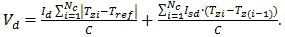
And one more technique applied for jitter measurement is based on use of time-voltage converter. Its block scheme is given in the Figure 10. It can be seen at once that measurement result is an average jitter.

Figure 10. Measurement circuit
The measuring system consists of charge pumping, logical element “XOR”, analog comparator with hysteresis, a condenser, D-trigger and binary scaler with digit capacity count of four. Signal jitter measurement from the output VCG is not made directly. For measurement it uses PLL reference signal as a standard one. As it is known frequency-phase detector of PLL system forms an error pulse with the length proportional to phase difference of two signals at input. Therefore, if we measure width of pulse at PFD output, it is possible to calculate the size of temporary jitter of VCG output signal. Let us consider scheme operation in dynamics.
Reference signal Sref and output signal of D-trigger Vcmp are controlled in the charge pumping by the keys S1 и S2, accordingly, when pulse-jitter at XOR output and signal from inverted output of D-trigger Vncmp is controlled by the keys S3 and S4, one-by-one. Charge out output is connected to negative output of analog comparator. Voltage source Vcent, which is connected to positive output of the same analog comparator sets central voltage of hysteresis. Source voltage value Vbase corresponds to the lower limit of comparator voltage. Thus, in the process of measurement charge and discharge process will start and finish exactly in this voltage point.
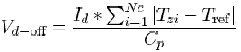
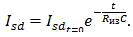
As soon as measurement procedure starts VIIN is less than Vcent in the initial position, and accordingly logical "1" is set at inputs and outputs of comparator VCP and D-trigger. At the same time signal at D-trigger output closes the key S2. And also reference signal Sref closes the key S1 in the first positive half cycle. And then condenser charging process with Ic current starts. As soon as voltage at comparator negative output reaches maximum threshold value VIH=2Vcent+Vbase, VCP will switch to logical "0". With next front edge delivery of Sref, D-trigger output signal will set on "1", аn inverted output – on "0". Thus, S2 opens and condenser charging process stops. Current source values Ic and condenser capacity С are required to be chosen in such a way so that charging process to last exactly for one cycle Sref . Just after Vncmp switches to logical “1” condenser discharging process starts and simultaneously pulse number readout of Sref activates during this process. As soon as jitter-pulse emerges at the output of frequency-phase detector, key S3 closes and condenser С starts to discharge with current Id, and voltage at analog comparator output will fall to VIL, thereafter Vncmp will switch from logical "1" and key S4 opens, i.e. charging process will finish. At this time pulse number Nc read by binary scaler is delivered to the output. Then it is possible to define long-term jitter value of VCG output signal by processing the data obtained. The Figure 11 shows time charts of measuring set operation.

Figure 11. Time charts
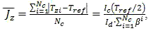
Mathematically operation of the measuring set can be considered in the following way. With coefficient of charge of Sref being equal to 50% of positive period duration amounts to Tref/2. During charge process, in the first half period, voltage at condenser is defined according to the following formula:
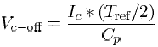
And in the process of discharge
As these two abovementioned voltages are equal to each other in the measurement process, by making them equal we shall obtain the following
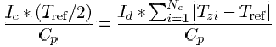
Wherefrom,
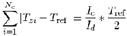
Thus jitter amplitude averaged value will be
One of advantages of this technique is in the fact that by charging one and the same condenser we avoided the necessity to use high-accuracy condensers, that is practically not realizable. This approach is also effective as it excludes exhausting process of condenser adjustment. Moreover, the method does not need synchronization. As was said above clock signal frequency, as minimum, must be by an order higher than frequency of the signal being measured, and use of time-voltage converter allowed us using the signal, frequency of which is by an order less than of the jitter itself. Despite it the method has a range of disadvantages. The following belong to them:
• Leaks while setting currents Ic and Id
• Leaks at condenser connected with condenser self-discharge
• Delays brought by PLL frequency-phase detector
• Complexity of counter selection
In the next chapter we shall consider quality parameters evaluation of each method. As well as possibility of methods’ improvement.
Evaluation of method’s quality parameters. Improvement of methods.
1. Discrete count method
To analyze this method measurement accuracy we shall use one of the most known methods described below.
For the abovementioned method to be accurate enough, time interval tx being measured should be significantly higher than
the period of clock generator Тc. If tx becomes comparable to Тc value, significant error of measurements appears. It is
explained further why it happens.
Let

where a is a whole number, and b is a proper fraction. Figure 12 shows counting pulses at b≤1/2, i.e. it is assumed that sequence of clock pulses has 50% charge ratio. It can be seen in the Figure 12 that if event А happened at time moment tА being in АВ interval, the number of counted pulses will amount to( a+1), and if tА is in BC interval, number of pulses will amount to a.

Figure 12. Error of time measurement
In this case measuring error can be defined in the following way:

For b≥1/2 it can be similarly written
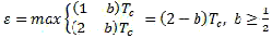
As it can be seen measuring accuracy directly depends on CPG, i.e. the higher the frequency the more accurate the measurement is.
While measuring jitter of SHF signals this method is ineffective. It is connected with complexity of high-frequency CPG realization. This problem can be solved by means of using frequency dividers at output of measuring set or at output of the source for which jitter is measured. For example, to measure jitter of PLL output signal there is given a model of PLL system [6] with dividers connected in a special way at its output allowing to transfer the measured signal from the high frequency to the lower one (Figure 13) to simplify jitter measurement.

Figure 13. PLL system with dividers at output
2. Method of time interval conversion into voltage unlike discreet count method is more effective while measuring jitter of high-frequency signals.
In the foregoing chapter above there were shown the main disadvantages of this method. Let us consider influence of these disadvantages on measuring accuracy.
1. Measuring accuracy connected with leaks while setting currents Ic and Id
Resulted from (10) any leaks while setting currents Ic and Id influence jitter measuring accuracy. Setting the condition that currents Ic and Id initially were set with an accuracy of ∆Ic and ∆Id, accordingly, where |∆I|< I, then (10) can be written in the following formula:
Then relative error will be defined in the following way:
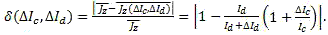
Let us note that errors while measurement do not depend on absolute values of currents Ic and Id, though depend on relation of currents Ic/Id, as pointing to advantage of this measuring method.
2. Measuring error connected with disadvantages of PLL frequency-phase detector.
Phase detector shortcoming is its having a dead zone, i.e. it is a phase error not detected by phase detector. At this time dead zone of high-quality phase detectors makes 15 ps [7]. Thus jitter with amplitude of not less than 15 ps is impossible to be measured in this way.
3. Measuring errors connected with leaks at condenser
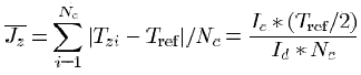
In reality condenser is not capable to maintain voltage with time flow. To some extent accumulated charges are lost on it, i.e. self-discharge process is observed.
Condenser self-discharge takes place according to the following
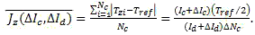
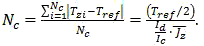
Then condenser discharge will have the following formula:
As jitter amplitude is much less then the period of reference signal Tref, it can be suggested that Tzi-Tz(i-1)=Tref/2. Now having solved the equation (8) in relation to (19), and after additional calculations we shall finally obtain:
where,

Then relative error according to formula (15) will be:
As can be seen from the last formula the more qualitative the condenser is, the less measuring errors are.
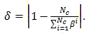
4. Measuring errors connected with counter digit capacity
If we express counter digit capacity Nc from (10), we shall get the following:
Increasing relation Id/Ic we similarly can decrease Nc, which from the one hand will result in reduction of measuring time, and other hand – to deterioration in device resolving power. That is why it is necessary to choose such a relation of currents for the error to be minimal.
Let current ratio value Id/Ic was taken by k1 more, then accordingly Nc will be by nc1 values less. Then we have:
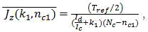
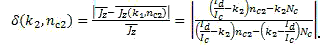
And, accordingly, when Id/Ic is by k2 less, Nc is by nc2 more:
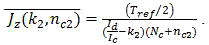
Let us find relative error for each case. It will be as follows, accordingly:
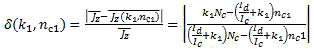
and
Conclusion
As a part of work there were considered several main methods of jitter measurement specifying advantages and disadvantages
of each of them. There were also given recommendations as for method improvement.
Further work intends execution of analytical analysis for measuring errors of methods. As well as realization of digital
modeling of measurement facilities realizing the method in accordance with developed structure and working out of
recommendations as for creation of jitter measuring sets, methods and techniques of measurement.
References
1. Бакланов И.Г. Технологии измерений в современной телекоммуникации. – м.: Эко-Трендз, 1998. – 264 с.
2. Mike Peng Li. Jitter, Noise, and Signal Integrity at Hight Speed. – Prentice Hall – 2008. – 368 pg.
3. Либацкая О. Н. Исследование взаимосвязей в кабельных линиях как причин
возникновения джиттера в цифровых системах передачи. – Автореферат магистра ДонНТУ.
http://masters.donntu.ru/2005/kita/libatskaya/diss/index.htm
4. Горшков А. П. Апаратура для частотных и временных измерений. – М: Советское радио -1971. – 336 с.
5. Tian Xia, Jien-Chung Lo. Time-to-voltage converter for on-chip jitter measurement. – IEEE Transactions on instrumentation and measurement – 2001. – 11 pg.
6. Tsan-Huei Wu. Low-cost jitter measurement technique for phase-locked loop – Thesis for master science, 2004, 90 pg.
7. Dean Banerjee. PLL Perfomanse, Simulation, and Design, Fourth Edition, 2006. – 339 pg.
8. Wolfgang Maichen. Digital Timing Measurement. – Netherlands: Springer, 2006. – 250 pg.
9. John A. McNeill, David Ricketts. The Designer Guide to Jitter in Ring Oscillators. – USA: Springer, 2009. – 292 pg.
10. Mhd Zaher Al Sabbagh, B.S. 0.18μm phase / frequency detector and charge pump design for digital video broadcasting for handheld’s phase-locked-loop systems . – Thesis – 2007, 44 pg.
http://etd.ohiolink.edu/send-pdf.cgi/Al%20Sabbagh%20Mhd%20Zaher.pdf?osu1196281141
Note – For the moment of compiling this author's abstract the Master’s qualifying paper has not been completed yet. Date of final work completion: December 20, 2010. Full text of the paper and materials to the subject matters can be obtained from its author’s or his research advisor after the specified date.