Analog Automatic Test-Pattern Generation
Ramadoss and Bushnell [533] proposed structural analog circuit testing, where they generate test waveforms that verify which component values or ratios of component values are within specifications. This method shortens tester time per circuit, by reducing the number of measurements.
They targeted analog/mixed-signal circuits [533] with these characteristics:
• They are linear, first-order blocks designed using signal flow graphs (SFGs.) These are cascaded to realize second-order transfer functions.
• The analog part lies on the chip inputs and feeds the digital block after A/D conversion. The digital part may/may not have independent primary inputs (PIs.)
• The analog part is observable only at digital or analog outputs.
This important circuit class has applications in filtering and amplification. Circuit blocks can be cascaded to achieve a required transfer function, and are easily designed using SFGs. Unfortunately, integration of analog and digital circuits on the same chip reduces controllability and observability. One cannot sensitize the fault in the digital sense as there are an infinite number of faulty values; however, the range of good values is known.Ramadoss and Bushnell provide this test generation solution [534]:
1. A user-specified output measurement tolerance leads to good and bad output values defining an output waveform envelope. They work backwards from the analog/digital interface with these values to generate structural analog component tolerances (or component ratio tolerances) that guarantee meeting the output specification. This process is the analog backtrace.
2. The key element in analog backtracing is working backwards through the analog circuit, i.e., reverse simulation, to calculate the input test given the output(s.) They use SFG inversion and backwards traversal to compute (from digital testing requirements) corresponding analog test input waveforms, which excite fault(s) and propagate faulty analog signals through the analog and digital parts to digital outputs (the analog backtrace.) This is done for each path from input to output in the circuit SFG.
Signal flow graphs represent the circuit input-output relations in graph form, and our analog backtrace method over the inverted SFG is analogous to digital test generation. When analog blocks drive a digital circuit through an A/D converter (ADC), one can backtrace from the digital circuit inputs to calculate the analog inputs needed to justify digital tests.
Reverse Simulation
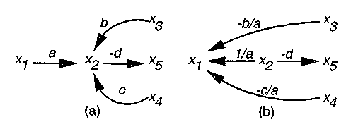
A signal flow graph (SFG) graphically represents the set of equations relating circuit state variables, inputs, and outputs of an active network circuit. Nodes can be source nodes, with outgoing edges only; sink nodes, with incoming edges only; or both. The value of any graph node (state variable) i is:value(i) = SUM(parent_node_value) * (incoming_edge_weight)
Consider the following equation with its corresponding SFG in Figure 11.9(a):
x2 = a*x1 + b*x3 + c*x4 (11.37)
x5 = -d * x2
Only incoming edges effect the value of a node, so has no effect on Node
Consider a rewritten version of Equation 11.37 and its SFG in Figure 11.9(b):х1 = 1/а * х2 - b/a * x3 - c/a * x4 (11.38)
They extended the path inversion algorithm of Balabanian et al. [61] to invert the path between an input and output of a SFG.
Figure 11.9: Signal flow graphs of (a) Equation 11.37 and (b) Equation 11.38.
Algorithm 11.1 Signal Flow Graph Inversion Algorithm.
1. Select a path in the SFG from PI through intermediate nodes through to2. Start at the primary input a source node with only outgoing edges.
3. Reverse the direction of the outgoing edge from to and the new weight 1/a is the reciprocal of the old weight a. becomes a sink node (with incoming edges only.)
4. Redirect all edges incident on to multiply the original weights by the new weight 1/a on the reversed edge from to and change the sign.
5. Repeat Steps 3 and 4 for all source nodes on the path from to PO until becomes a source node. At this point, since all of the graph edges point towards the input, the graph is inverted.
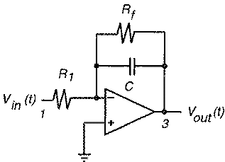
Figure 11.10: Real integrator circuit.
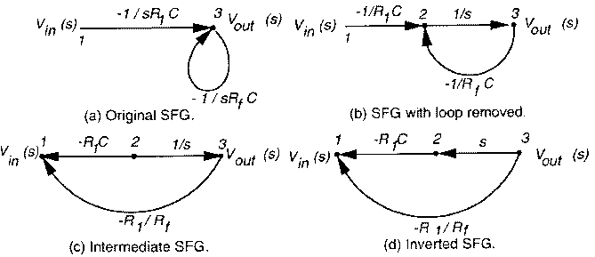
Example 11.2 Consider the integrator circuit in Figure 11.10, its signal flow graph in Figure 11.11, and the equivalent Equation 11.39:
(11.39)
Nodes 1 and 3 of the SFG correspond to the circuit voltage input and output, respectively. Figure 11.11(a) shows the original SFG of the integrator, with a self-loop on the output. Node 2 in Figure 11.11(b) is a dummy node introduced to avoid a self-loop on the output node – it has a weight of 1/s that was common to both edges in the original graph. Differentiation (represented by the s operator) is a linear operation. Hence, multiple edges with non-zero s weights in the SFG of a single first-order block can be combined to produce multiple edges with ordinary numerical weights and one edge with non-zero s weight. This helps in reverse simulation, as numerical differentiation, an expensive operation, is done only once.
After Steps 3 and 4 of the algorithm, we have the intermediate SFG in Figure 11.11(c). The edge with weight -1/R1C has been reversed and its new weight is now -R1C. The edge from the output, with weight -1/RfC has been redirected to the input node, and its new weight is -(-R1C * -1/RfC) = -R1/Rf. Only one more edge need be inverted: the intermediate edge to the output with weight 1/s. It is inverted with the new weight becoming s; at this stage we stop, the output having become a source node and the input a sink node. Figure 11.11(d) shows final inverted graph and is equivalent to the equation:
Vin(s) = -R1C * s(Vout(s)) - R1/Rf*Vout(s) (11.40)
All cycles in the original SFG are broken in the inverted graph, which is now a feedforward network. All of node i’s parents in the inverted graph will be closer to the circuit output than i. In SFGs, input and output are merely labels, and are interchangeable.
Figure 11.11: Original and modified signal flow graphs of the integrator.
One can simulate the inverted SFG with a chosen output to find the original network input. The s operator in the Laplace domain corresponds to differentiation in the time domain. The process starts with a set of output samples. The inverted graph weights are all either numerical scalars or s, the differential operator that can be numerically approximated. One can find all inverted graph node values using Equation 11.36. This process finds the input corresponding to a given output, but non-linear networks must have an non-linear block input constrained to a constant before a SFG can be built for reverse simulation. One may have to search among many possible constant inputs to find an acceptable test. This provides a new ability to work backwards in an analog circuit during test generation. The method takes a set of actual SPICE output samples and uses them to reverse simulate the original circuits in the time domain. Most samples were equally spaced points apart in time.
Analog Backtrace
The reverse simulation algorithm can be used to define faults and generate analog circuit test waveforms. One starts with an output waveform tolerance, and works 11.6 Analog Automatic Test-Pattern Generation 411 backward with good and bad outputs. The good input found is the test signal, and the bad output and node values calculated along the way let one calculate component deviations.
Test Generation Algorithm:
1. The user sets a circuit output voltage magnitude tolerance.
2. Parse the netlist (in SPICE format), build the SFG, and store edge weights symbolically as well as numerically.
3. Invert the SFG using Algorithm 11.1 and store edge weights numerically and symbolically.
4. Obtain a set of samples of the good machine output.
5. Perform good output reverse simulation and find values at all nodes, including the primary input (for all samples.)
(a) Apply the good output waveform sample to the PO.
(b) Traverse the SFG backwards from the PO in breadth-first order, setting all intermediate node values numerically using Equations 11.36 and a second-order approximation to the differential s operator [80]. If the inverted SFG has loops, iterate until signals converge.
(c) The PI now has the correct good machine test waveform.
6. Perform bad output reverse simulation as in Step 5 and find all bad machine node values.
7. Calculate all internal structural component tolerances, either for single components or ratios of multiple components, using the method below.
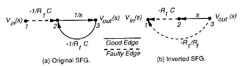
Figure 11.13: Original and inverted SFGs for integrator.
Summary
Analog circuit fault simulation and automatic test-pattern generation methods based on fault models are beginning to gain limited acceptance in industry. A recent panel concluded that these models will now begin to augment the traditional functional, DSP-based analog tests that are derived without reference to a fault model [346]. The advantage of the fault models is the opportunity to shorten the number of tests, which is now important for reducing testing costs. Also, analog fault models allow computation of a fault coverage for analog circuit testing, which is also attractive. The factors that are increasing the costs of analog testing, and forcing the investigation of new methods, are the widespread advent of mixed analog/ digital circuits, which have significantly raised testing costs, and the advent of higher precision, 22-bit converters, for which conventional testing methods are too expensive.