
Abstract
Table of contents
- Introduction
- 1. The structure of the cache in the microprocessor system
- 2. Simulation of cache memory with the help of the stand EV8031/AVR
- Conclusion
- References
Introduction
In modern computer systems used throughout the operation caching. Ideas have cached a long time and developed so far. Caching is used CPUs, hard drives, web browsers, web servers, DNS and WINS.
Cache - a memory with higher speed access designed to accelerate access to data contained in the permanent memory at a lower rate of access (the "main memory"). The cache consists of a set of records. Each entry is associated with a data item or data block (a small piece of data), which is a copy of the data item in main memory. Each entry has an identifier that defines the mapping between data elements in the cache and their copies in the main memory [1],[5].
The cache memory can have several levels, has a different structure and algorithms.
Since the principle of the cache is almost the same in any system with cache, then develop a model of the cache controller can simplify the study of algorithms and the structure of the cache, and should allow to evaluate their effectiveness.
It is known that the speed of the microprocessor is much higher than the speed of main memory[7]. In view of the fact that the bus does not allow data to work with high frequency, this memory must be located close to the microprocessor itself. This imposes a significant limitation on the amount of memory and significantly increases the cost. Because, basically, manufacturers produce a slow but cheap memory with a lot of justifiable use of multi-level memory.
But there is also a technology that combines the work of fast memory with slow, resulting in a memory with a relatively high speed of work and large capacity. Memory of a small amount of high-speed operation is called a cache.
Cache memory is one of the upper levels of memory hierarchy between the general purpose registers and random access memory. The speed of the cache memory is comparable to the speed of the microprocessor. Memory hierarchy with two levels of cache memory is shown in Figure 1 [1].
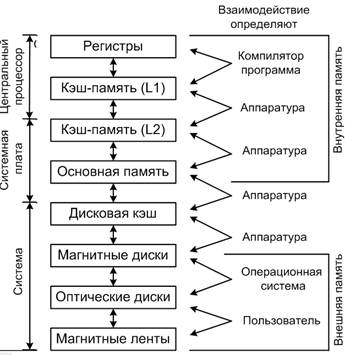
Figure 1 – Hierarchy of memory in the microprocessor system
The idea of using a fast buffer memory between the CPU and main memory appeared long ago in the IBM System/360, it has been used is not the first time. The Soviet computer function performed cache memory for ultra-fast registers, which are also located between main memory and the processor is an example of BESM [2]. The cache uses a small, very fast memory (usually a type of SRAM).
The main idea of the cache - is deposited with the words most often used. If the microprocessor to a word processor first checks the cache. And only if there is no word, refers to the main memory. If a large part of the requested word is located in the cache, the average memory access time is significantly reduced. Sometimes an appeal to the main memory cache in parallel, while in the case of cache hit main memory address to be terminated. Structural scheme the location of the cache is shown in Figure 2.
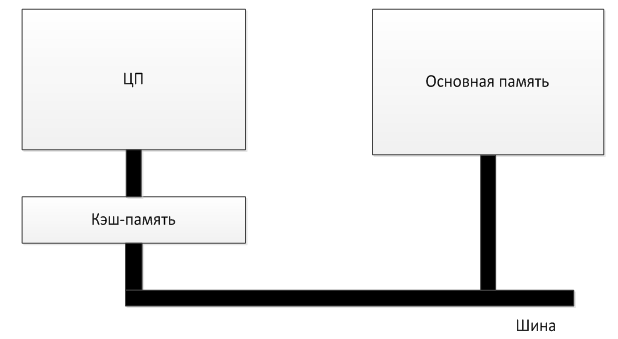
Figure 2 – Structural scheme the location of the cache
The success or failure of the operation to access the cache memory is called a cache hit (hit ratio) or a cache miss (miss ratio) [3]. These operations are directly dependent on what the words are in the cache. A well-known fact is that the programs do not address the memory in the spread. Often, after a short address, and a very high probability we can assume that the next wakes up an address in the address A. The vast majority of commands are used in the regular program called from sequential memory locations. Just know that most of the time of execution of the programs take the same type of sets of commands that are executed in a loop [7].
Figure 3 – The work of the cache
(Animation 12 frames, 7 loops, 14.2 Кб)
The basis of all systems of the cache is the principle of locality. This is when a sequential memory access within a certain time is only part of it. The idea is that when referring to a word of it, along with neighboring transferred to the cache memory, which can quickly turn to them when prompted [1].
In the classic version, there are two levels of cache memory - the first and second level. The third level of organization is different from the second level cache. If data are not processed or processor must process the urgent data, for the release of the second level cache memory data is moved to the cache memory of the third level. Also, the cache in the third level in the multi-core processors is used to exchange data between the cores. Sometimes it is used and the cache memory of the fourth level, but its use is justified in servers and mainframes. With regard to the introduction of the memory of this level of general purpose microprocessors is a discussion [6],[4].
Another cache memory can be integrated (unified cache) or divided (split cache). The combined stores as well as team instruction. (U-cache). In a split cache instruction cache exists (I-cache) and data cache (D-cache). This allows parallel processing of data and commands. In the majority of processors is divided by a cache of the first level. A cache of the second and third level are unified. Sometimes the cache in the third level is called T-cache (ternary - tertiary). The structure of the location of the cache of different levels of Figure 4.
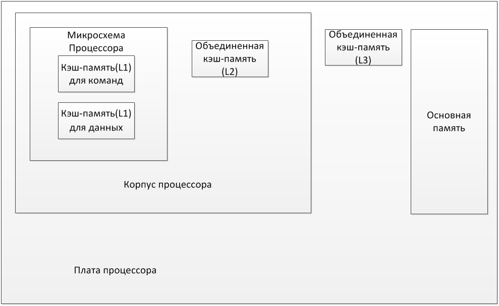
Figure 4 – Example of the location of the cache with three levels
The advantage of a mixed cache is that for a given volume, it is characterized by a higher probability of hits, compared to a split, because it automatically sets the optimum balance between instructions and data. If the executable code fragment access the memory associated mainly with the sampling instructions, and the proportion of accesses to the data is relatively small, the cache memory has a tendency to fill the instruction and vice versa.
The advantage of the Partitioned cache is that the operation can begin independently in both types of cache, thus avoiding possible conflicts. Such parallel processing doubles the bandwidth of the memory system. Yet it is worth noting that each cache (such as - I-cache and D-cache) has independent access to main memory.
2. Simulation of cache memory with the help of the stand EV8031/AVR
Simulation of cache direct mapping (single-channel cache). Cached memory area is divided into blocks whose size is equal to the amount of cache memory. Address of cache lines, which displayed a block of main memory, which is uniquely determined by the expression: i = j mod m, where m - the total number of rows in the cache.
A cache direct mapping - a simple type of cache, effectively used in instruction cache (I-cache).
The advantages of cache direct mapping are:
- High-speed determining hit / miss,
- Easy to search for a string of a candidate for deletion, as there is rigid adherence to the addresses.
The main drawback - low efficiency in the structures of D-cache, because at the same time you can put one set only one line, despite the presence of irrelevant strings to other addresses. Consequently, the simultaneous processing of multiple segments, equally spaced in different pages of memory (for example, the multiplication of two arrays in pairs), the controller can initiate a further exchange of data between main and cache memory.
The model is implemented memory size of 16 bytes and the cache line size of 1 byte with four strings. Thus, the zero line of the cache memory bytes may correspond with the numbers 0,4,8,12, the first row of numbers 1,5,9,13, etc. At the same time in the cache data is stored in addition to the tag that points to a memory location is mapped to the currently active line of the cache. The structure of the cache direct mapping [5],[1] is shown in Figure 5.
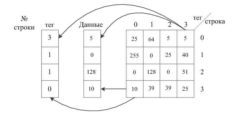
Figure 5 – The structure of the cache direct mapping
Record line in the cache memory is accompanied by an entry in the memory tag number of the pages of main memory.
With this structure, the main memory address can be viewed as consisting of three parts: the page number, otherwise known as a tag line number in the page, otherwise known as the index number of bytes in the string. Consequently, the control device is known in advance the address data stored in the cache.
The model is implemented in the write-back mode cache (WB - Write Back). To point to the fact of change line without copying it into the main memory is a sign of modification M (Modified). The line with the sign of M does not correspond to the mapped cell content of main memory. Tag is reset to zero at the initial loading line in the cache memory and is set to one when writing the updated row. Thus, to ensure the coherence of the data to overwrite the main memory only needs a single string value of the attribute modification. Write-back mode is rational, but the time difference allows the data cache and main memory.
When reading from memory into the cache line is marked with a sign S (Shared), which indicates that full compliance with the contents of memory. Cache lines that do not contain reliable information, marked with a sign I (Invalid), a reference to the row leads to cache misses.
To specify each attribute is assigned one bit, the tag - 3 bits. The structure of a cache line is shown in Figure 6.
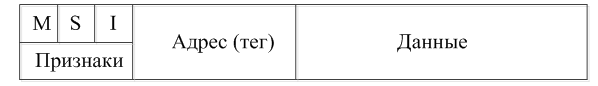
Figure 6 – The structure of a cache line
With LED indicator line static stand displays the results of exchange with the main memory. LED indicates the line of the cache hit (LEDs light up) when the cache miss Tally no. In a static indicator output data read from memory, which allows you to check their correctness.
The model allows to evaluate the effectiveness of cache direct-mapped write-back, which is calculated ratio of cache hits. As a baseline amount of cash received and the total number of hits references to the word in memory. For example, the word at address A had 15 hits, 10 of them had just a fact of cache hits. Thus, the coefficient is equal to 10/15 = 0.66, which indicates that 66% of cache hits.
As a consequence, we can calculate the index of the average data access time:

We assume that the response time of cache memory 2 microseconds, and the time to access main memory 200mks, while the coefficient of cache misses is equal to 3%. Consequently, the average access time will be equal to 2 + 200 * 0.03 = 8 ms.
Conclusion
In microprocessor-based systems, the cache is used by computer standards, a very long time. The beginning of its use was associated with low-speed main memory. And the basic idea of its operation have not changed so far. Modern cache can work with a speed comparable to the CPU (L1).
Gradually there is a tendency to increase the number of levels of cache memory. Since even a fourth level cache works several times faster than the primary. Although in practice until the applicable three-tier structure of the cache. Also, it was determined that since most systems are efficient pipelining of the first level of a distributed cache that can improve the performance of exchange with the main memory of up to two times.
Master's thesis is devoted to actual research work to investigate the problem of cache memory. And to develop a model of the cache controller with stand EV 8031.
- Implemented on a model stand cache allows to study in detail mode with write-back, and see the advantages and disadvantages of cache direct mapping.
- Based on the analysis of the literature highlights the main algorithms for the cache.
The work on the magister's work is in progress. The following task will be to implement interaction with stand and support more cache algorithms.
References
- Таненбаум Э. Архитектура компьютера / Таненбаум Э. – Питер, 2010. – 5е издание. – 844с.
- Королев Л.Н. Архитектура ЭВМ БЭСМ-6 [Электронный ресурс]. – Режим доступа: http://www.parallel.ru/history/besm6.html
- Касперский К. Кэш-память, как она есть [Электронный ресурс]. – Режим доступа: http://www.insidepro.com/kk/008/008r.shtml
- Пахомов С. Долгожданные процессоры с микроархитектурой AMD K10/Пахомов. – КомпьютерПресс 10'2007
- Гук М.Ю. Апаратные средства IBM PC. Энциклопедия / Гук М.Ю. – Питер 2006. – 1072 с.
- Anand Lal Shimpi The Cache Debate, LGA-1156 and the 32nm Future [Электронный ресурс]. – Режим доступа: http://www.anandtech.com/show/2671
- Жмакин А.П. Архитектура ЭВМ /Жмакин А. П. - СПб. – 2006 – С. 259