![]()
|
|
Keith H. SuekerPower Electronics Design: A Practitioner’s GuidePulse Width Modulation.Source: Keith H. Sueker Power Electronics Design: A practitioner's Guide, © 2005, SciTech Publishing Inc. |
![]()
Introduction.
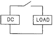
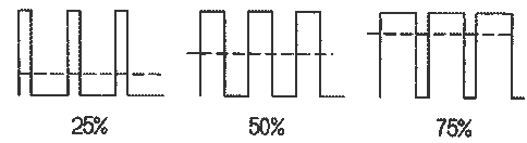
If the DC supply shown in Fig. 1 can be switched rapidly on and off, the load waveforms will be those shown. A continuously variable average voltage from (nearly) zero to (nearly) the full supply voltage is available by changing the duty cycle of the switching. The “nearly” has to be added, because switching devices in the real world have minimum on times that produce a small output and minimum off times that prevent them from reaching full output voltage in a controlled manner. They can be switched completely on or completely off, but small prohibited areas of control always exist near those extremes.
a)
b)
Figure 1 Basic pulse width modulation.
The limitations imposed by the need
for AC line voltage or forced commutation in SCRs limited their applications
in pulse width modulated systems, and they spurred the development of SCR derivatives
that could be turned off by a control signal. The SCR morphed in one direction
into the gate turnoff thyristor (GTO). This device can be turned off by a gate
signal with a very high peak power but a small average power. The GTO is available
in high-current and high-voltage ratings and has found niche applications where
its characteristics are favorable. But it remains very expensive, and it cannot
be classed as a general-purpose industrial control device at this time.
Another SCR derivative is the integrated gate controlled thyristor
(IGCT). The IGCT can interrupt anode current by having a current larger than
the anode current injected into the gate. It requires a very low inductance
in the gate circuit to create a current equal to the anode current with a low-voltage
supply, and that mandates incorporating the gate driver into the physical packaging
of the IGCT. The required energy storage for the gate signal is aided by the
use of “supercaps,” low-voltage electrolytic capacitors with a very high energy
density. Again, the device is not really suitable for general-purpose use, although
it has been used successfully in high-power applications. Both the GTO and the
IGCT are somewhat handicapped by the regenerative, latching characteristic of
the parent SCR. They do not cease conduction gracefully but must be driven out
from the gate. Developments on power transistors continued through the years
and resulted in a breakthrough when a field effect transistor was wedded to
a conventional bipolar transistor. The result, the integrated gate bipolar transistor
(IGBT), is rapidly becoming the device of choice for many applications. It has
engendered a host of new high-power equipment designs featuring switchmode operation.
The device has the ability to operate at frequencies several orders of magnitude
higher than the SCR, although the higher-power IGBTs are more limited in their
maximum frequency.
The IGBT has a PNP power transistor
controlled by a field effect transistor such that it has the best properties
of each. It can handle very high powers and yet be controlled by a gate that,
being insulated and field controlled, draws no current. Figure 13.2 shows the
collector-emitter voltage as a function of the collector current for several
different gate-emitter voltages. As the gate voltage is increased, the IGBT
begins to draw current, and this current increases with collector voltage until
a region is reached at which the current is constant for a given gate voltage.
At high levels of gate voltage, however, a saturated region is reached in which
the collector-emitter voltage varies only slightly with collector current. Although
the IGBT can be operated as a linear amplifier in the same manner as a transistor,
it is almost always operated as a switch between off and on with enough gate
drive so it remains at the lowest possible voltage drop for the required current.
The saturated voltage drop is typically in the 3.0-V range. IGBTs are currently
available in voltages to 6000 V and currents to 2000 A. Most large IGBTs are
packaged in a molded plastic assembly on an integral mounting plate that serves
as a contact medium to a heat sink. The active device itself consists of a large
number of small IGBTs connected in parallel with bond wires to the external
electrodes. Many have an integral inverse parallel diode.
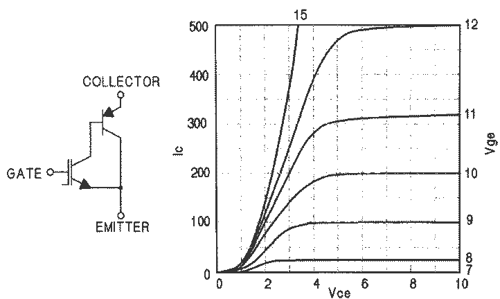
Figure 2 - IGBT schematic and characteristics.
External circuitry for the IGBT must
recognize the fast switching characteristics of the device. Turn-off time can
be as little as 500 ns and, with collector currents as high as several thousand
amperes, the circuit di/dt can reach fearsome levels. It is imperative that
stray inductances in snubber circuits be kept to an absolute minimum to protect
the device from overvoltage. It is also necessary to prevent excessive load
current from pulling the IGBT out of saturation. The dissipation will rise to
high levels that can destroy the device in a relatively few microseconds. Yet,
immediate cessation of gating may create an excessive di/dt and an overvoltage
on turn-off from faults. The designer must balance the need to limit dissipation
with the need for voltage protection by controlling the rate of gate signal
turn-off.
Lest one conclude from the above that the IGBT
is a fragile device, nothing could be further from the truth. IGBTs have proven
themselves as the power conversion elements in AC motor drives over 20,000 hp
and in choppers for DC electric arc furnaces at power levels above 100 MW. They
are rugged, reliable devices.
Four IGBTs can be combined to form a bipolar switching circuit that is the basis for many motor drives and other applications. Figure 3shows the basic H-bridge. The IGBTs are each equipped with an antiparallel diode that provides a free-wheeling path for load current and clamps any switching transients to the DC buses. If IGBTs 1 and 2 are turned on, load current flows in the direction of arrow F. If 3 and 4 are on, the current flows in direction R. Both polarities can be pulse width modulated to form an AC output waveform.

Figure 3 - The “H” bridge.
If a sine wave is used as a command waveform, the switching series is shown in Fig. 4. The output waveform will be somewhat “ragged,” because the switching frequency is quite low to illustrate the process more clearly. The output waveform is sometimes cleaned up with an output filter to lessen harmonics at the load.

Figure 4 - PWM sine wave switching.
The proper switching protocol is essential
to operation of the “H” bridge. If, say, IGBTs 1 and 2 are switched on at the
same time that 3 and 4 are switched off, there will be a short circuit
because of the turn off times of 3 and 4. An “underlap” circuit is necessary
to ensure that 3 and 4 are turned off and recovered some time before 1 and 2
are turned on.
One more section can be added to this
circuit to form the threephase motor drive shown schematically in Fig. 5.
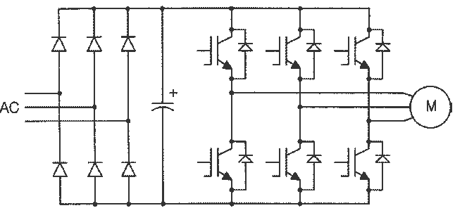
Figure 5 - IGBT motor drive.
Many variations on the three-phase circuit have been devised to meet the objectives of lower harmonic distortion at the load, higher voltage output, and a host of other specialized needs. One objection to the basic H-bridge is that the load is switched from peak positive voltage to peak negative, and alternative circuits have been developed to provide lower voltage switching steps to reduce the dv/dt at the motor. Among these circuits is the neutral-point-clamped inverter, an arrangement that offers five switching voltage levels instead of only two. In addition to the size of the voltage step, the dv/dt tends to rise with the switching frequency, because the higher-frequency semiconductors switch faster. Motor windings are subject to the front-of-wave effects, and the application of solid-state drives to older motors led to problems with insulation failures. Motor manufacturers developed enhanced insulation techniques, and motors are now available that are rated for solid-state drives. Various types of transistors can be used in the basic H-bridge to operate directly from the AC line and power a high-frequency transformer. Small, lightweight, high-frequency transformers and filters have revolutionized the design of DC power supplies for all manner of equipment operated from a 120-Vac line.