|
http://www.analog.com/UploadedFiles/Data_Sheets/ADSP-2185.pdf ADSP-2185Information furnished by Analog Devices is believed to be accurate and reliable. However, no responsibility is assumed by Analog Devices for its use, nor for any infringements of patents or other rights of third parties which may result from its use. No license is granted by implication or otherwise under any patent or patent rights of Analog Devices.
This data sheet provides a general overview of ADSP-2185 functionality. For additional information on the architecture and instruction set of the processor, refer to the ADSP-2100 Family User’s Manual. For more information about the development tools, refer to the ADSP-2100 Family Development Tools Data Sheet. ARCHITECTURE OVERVIEW The ADSP-2185 instruction set provides flexible data moves and multifunction (one or two data moves with a computation) instructions. Every instruction can be executed in a single processor cycle. The ADSP-2185 assembly language uses an algebraic syntax for ease of coding and readability. A comprehensive set of development tools supports program development.
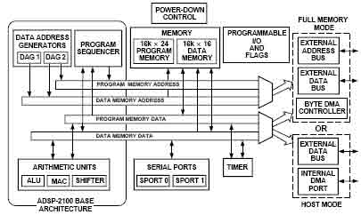
The two address buses (PMA and DMA) share a single external address bus, allowing memory to be expanded off-chip, and the two data buses (PMD and DMD) share a single external data bus. Byte memory space and I/O memory space also share the external buses. Program memory can store both instructions and data, permitting the ADSP-2185 to fetch two operands in a single cycle, one from program memory and one from data memory. The ADSP-2185 can fetch an operand from program memory and the next instruction in the same cycle. When configured in host mode, the ADSP-2185 has a 16-bit Internal DMA port (IDMA port) for connection to external systems. The IDMA port is made up of 16 data/address pins and five control pins. The IDMA port provides transparent, direct access to the DSPs on-chip program and data RAM. An interface to low cost byte-wide memory is provided by the Byte DMA port (BDMA port). The BDMA port is bidirectional and can directly address up to four megabytes of external RAM or ROM for off-chip storage of program overlays or data tables. The byte memory and I/O memory space interface supports slow memories and I/O memory-mapped peripherals with programmable wait state generation. External devices can gain control of external buses with bus request/grant signals (BR, BGH and BG). One execution mode (Go Mode) allows the ADSP-2185 to continue running from on-chip memory. Normal execution mode requires the processor to halt while buses are granted. The ADSP-2185 can respond to eleven interrupts. There can be up to six external interrupts (one edge-sensitive, two level-sensitive and three configurable) and seven internal interrupts generated by the timer, the serial ports (SPORTs), the Byte DMA port and the power-down circuitry. There is also a master RESET signal. The two serial ports provide a complete synchronous serial interface with optional companding in hardware and a wide variety of framed or frameless data transmit and receive modes of operation. Each port can generate an internal programmable serial clock or accept an external serial clock. The ADSP-2185 provides up to 13 general-purpose flag pins. The data input and output pins on SPORT1 can be alternatively configured as an input flag and an output flag. In addition, eight flags are programmable as inputs or outputs, and three flags are always outputs. A programmable interval timer generates periodic interrupts. A 16-bit count register (TCOUNT) decrements every n processor cycle, where n is a scaling value stored in an 8-bit register (TSCALE). When the value of the count register reaches zero, an interrupt is generated and the count register is reloaded from a 16-bit period register (TPERIOD). Serial Ports The ADSP-2185 incorporates two complete synchronous serial ports (SPORT0 and SPORT1) for serial communications and multiprocessor communication. Here is a brief list of the capabilities of the ADSP-2185 SPORTs. For additional information on Serial Ports, refer to the ADSP-2100 Family User’s Manual. SPORTs are bidirectional and have a separate, double-buffered transmit and receive section. SPORTs can use an external serial clock or generate their own serial clock internally. SPORTs have independent framing for the receive and transmit sections. Sections run in a frameless mode or with frame synchronization signals internally or externally generated. Frame sync signals are active high or inverted, with either of two pulse widths and timings. SPORTs support serial data word lengths from 3 to 16 bits and provide optional A-law and m-law companding according to CCITT recommendation G.711. SPORT receive and transmit sections can generate unique interrupts on completing a data word transfer. SPORTs can receive and transmit an entire circular buffer of data with only one overhead cycle per data word. An interrupt is generated after a data buffer transfer. SPORT0 has a multichannel interface to selectively receive and transmit a 24 or 32 word, time-division multiplexed, serial bitstream. SPORT1 can be configured to have two external interrupts (IRQ0 and IRQ1) and the Flag In and Flag Out signals. The internally generated serial clock may still be used in this configuration. |