Source: 4th ESA Workshop On Millimetre Wave Technology and Applications, Espoo, Finland, February 15-17, 2006, http://lerma7.obspm.fr/~maestrini/Work/Publications_files/ESA-Workshop-2006.pdf
Hui Wang, Jean-Marc Rollin, Byron Alderman, Bertrand Thomas, Steven Davies and Alain Maestrini
Abstract
This paper describes the design of a broadband fixed-tuned 183 GHz sub-harmonically pumped mixer featuring an anti-parallel pair of planar Schottky diodes monolithically integrated on a 50 um-thick GaAs substrate. The circuit is about 4 mm long, 0.28 mm wide and is mounted in a waveguide block that includes waveguide matching elements at the Local Oscillator (LO) and RF frequencies. The mixer is expected to work efficiently in the band 160-190 GHz using only 2 mW of LO pump power, with a Double Side Band (DSB) conversion gain greater than -5.5 dB. Best performances obtained in simulations are a minimum DSB gain of -5.1 dB at 183 GHz. The circuit will be fabricated using the standard BES process of United Monolithic Semiconductors (UMS).
1. Introduction
Among the spectral lines that can be observed at millimeter wavelengths with heterodyne receivers to retrieve the vertical moisture profile of planets such as the Earth or Mars, the water vapor line at 183 GHz is certainly one of the most important. For heterodyne instruments dedicated to planetary and atmospheric science, very high sensitivity is not a critical issue; the best mixing element at room temperature is still a GaAs Schottky diode due to it low noise performances, it easy usage, and well controlled fabrication process. In the frame of oncoming projects for the Centre National d'Etudes Spatiales (CNES), a Schottky diode based sub-harmonic mixer at 183 GHz has been designed and is intended to demonstrate the feasibility of millimeter and submillimeter-wave receivers based on European Schottky diodes. Future space-borne instruments of CNES or the European Space Agency (ESA) will use these components.
2. Design of the 183 GHz mmic mixer
2.1. Planar Schottky Diodes Chip
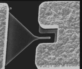
Our design is based on a preliminary study of the technology of UMS diodes [1]. Fig.1 shows a three-dimensional (3D) view of a Schottky diode from UMS with a single anode.
Fig.1 - View of a single anode Schottky diode from UMS
The diode is connected to the rest of the monolithic microstrip circuit with two side pads. The anode is connected to one of the pads with a surface finger tapered from the anode pad to the anode. The anti-parallel design configuration has been optimized for best SHP mixing performances including the anode size, as seen in Fig.2.
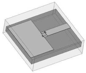
Fig.2 - The antiparallel diodes pair configuration inside the channel
The resulting electrical characteristics for each is an ideality factor η=1.2 , a saturation current ISAT=4.10-15A, and an estimated series resistance Rs=10Ω. A zero bias junction capacitance Cjo=2 fF is calculated based on the anode size and the epitaxial layer doping. 2.2. Circuit Optimization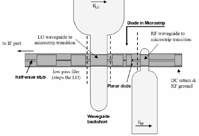
Fig.3 - Schematic of a mixer circuit inside a waveguide block
Wide E-probe waveguide-to-suspended stripline transitions are used to couple both the RF and LO signal into the channel. Reducing the height of both RF and LO waveguide in the vicinity of the E-probe transitions was found necessary in order to achieve broadband operation, as mentioned in [7]. Two low-pass stripline filters are used to prevent the RF signal from coupling to the LO waveguide and the LO signal to leak towards the IF connection.
3. Simulation results of the mixer performances
The performances of the whole mixer structure are computed with a harmonic balance code over the frequency range 160-200 GHz. The results are presented in Fig.4 for different values of LO input power.
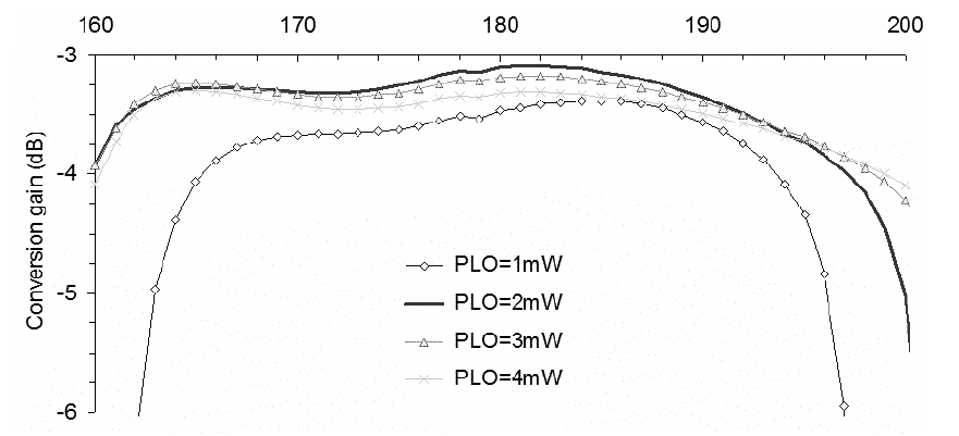
Fig.4 - Simulated performance of the mixer DSB conversion loss at 183 GHz with different LO power. Optimum mixer conversion losses are obtained for a LO power of 2mW. The IF frequency is set to fIF=4 GHz.
The expected DSB conversion losses are higher than -4 dB between 160 GHz and 196 GHz using 2 mW of LO power, with a best value of -3.1 dB at 183 GHz. Considering additional losses of about 2 dB due to the total conductor and dielectric loss of the horn and waveguide, as well as possible mismatches between the IF output of the mixer and the first IF low noise amplifier, the DSB mixer conversion loss is expected to be approximately 5.1 dB at 183 GHz.
4. Status of the circuit fabrication
A prototype of this mixer is currently being fabricated at the University of Bath in UK, using a process that allows the air-bridging of the diodes to decreasing the parasitic capacitances. This prototype shares the same chip-layout and waveguide block as the mixer designed for UMS BES process. Simulations show that the presence of air-bridges does not change significantly the matching of the diodes; therefore the same block is expected to be optimum for both circuits allowing a direct and relevant comparison between the two processes.
References
[1] A. Maestrini, "Report on the Evaluation of the Capabilities of the United Monolithic Semiconductors to Produce Schottky Diodes Based Mixers in the Band 100-380GHz", proceedings of the Round Table discussion on Schottky technology, ESA/ESTEC, Norrdwijk, The Netherlands, March 2004.
[2] B. Thomas, "Etude et réalisation d'une tête de réception hétérodyne en ondes submillimétrique pour l'étude des atmosphéres et surfaces de planétes", PhD dissertation, LERMA-Observatoire de Paris, France, December 2004.
[3] Advanced Design System, Version 2003A, Agilent Technologies, 395 Page Mill Road, Palo Alto, CA 94304, USA.
[4] J.L. Hesler, "Planar Schottky diodes in submillimeter-wavelength waveguide receivers", PhD dissertation, University of Virginia, Charlottesville, USA, Jan. 1996.
[5] High Frequency Simulation Software, V9.2, Ansoft Corporation, 225 West Station Square Drive, Suite 200, Pitts¬burgh, PA 15219, USA.
[6] A.V. Raisanen, D. Choudhury, R.J. Dengler, J.E. Oswald, and P. Siegel, "A novel split-waveguide mount design for millimeter- and submillimeter-wave frequency multipliers and harmonic mixers," IEEE Microwave and Guided Wave Letters, Vol. 3, No.10, Oct. 1993, pp.369-371.
[7] S.C. Shi and J. Inatani, "A Waveguide-to-Microstrip Transition with a DC/IF Return path and an Offset Probe", IEEE Transactions on Microwave Theory and Techniques, Vol.45, No.3, March 1997.