Abstract An RF amplifier is an active network that increases the
amplitude of weak signals, thereby allowing further processing by the receiver.
Receiver amplification is distributed between RF and IF stages throughout the
system, and an ideal amplifier increases the desired signal amplitude without
adding distortion or noise. Unfortunately, amplifiers are known to add noise and
distortion to the desired signal. In a receiver chain, the first amplifier after
the antenna contributes most to the system noise figure. Adding gain in front of
a noisy network reduces the noise contribution from that network.
Amplifier Noise Figure
To analyze the effect of circuit noise, one can model the
noisy circuit as a noiseless circuit plus external noise sources. For a noisy,
two-port network with internal noise sources (Figure 1a), the effects of
those sources are represented by the external noise-voltage sources Vn1
and Vn2, placed in series with the input and output terminals,
respectively (Figure 1b). Those sources must produce the same noise
voltage at the circuit terminals as the internal noise sources. The values of Vn1
and Vn2 are calculated in equations 1 and 2. Representing the
noise-free, two-port network in Figure 1b by its Z parameters:

and:

Equations 1 and 2 show that the Vn1 and Vn2 values can be
determined from open-circuit measurements in the noisy two-port network. It
follows from these equations that when the input and output terminals are open
(I1 = I2 = 0) (equations 3 and 4):

and:

In other words, Vn1 and Vn2 equal the corresponding
open-circuit voltages.
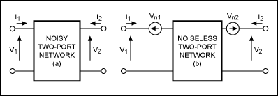
Figure 1. A noisy two-port network (a) can be modeled by a noise-free two-port
network (b) with external noise voltage sources Vn1 and Vn2.
In an alternate representation of the noisy two-port network (Figure 2),
the external sources are the current noise sources In1 and In2.
Equations 5 and 6 represent the noise-free two-port network:

and:

The values of In1 and In2 in Figure 2 follow from short
circuit measurements taken in the noisy two-port network, as shown in equations
7 and 8:
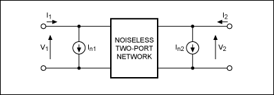
Figure 2. A noisy two-port network can also be represented by a noise-free,
two-port network with external noise-current sources In1 and In2.

and:

Other representations, besides those shown in Figures 1b and 2, can be derived
for a noisy, two-port network. A convenient representation for noise analysis
places the noise source at the input of the network (Figure 3).
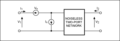
Figure 3. Again, a noisy, two-port network can be represented as a noise-free,
two-port network with external noise sources Vn and In at
the input.
Representing the noise-free, two-port network in Figure 3 by its ABCD parameters
in equations 9 and 10 show:

and:

Equations 9 and 10 show that there is no simple way to evaluate Vn
and In in Figure 3, using open- and short-circuit measurements. From
a practical point of view, those values (Vn and In) can be
expressed in terms of noise voltages Vn1 and Vn2 in Figure
1b (which require only open-circuit measurements).
The relationship between noise sources Vn and In in Figure
3 and noise sources Vn1 and Vn2 in Figure 1b is derived as
follows. Using Z parameters to represent the noise-free, two-port network in
Figure 3:

and:

Comparing equations 1 and 2 with equations 11 and 12, it follows that:

and:

Hence, solving equations 13 and 14 for Vn and In gives:

and:

An alternate method for determining Vn and In relates them
to noise sources In1 and In2 in Figure 2. It is easy to
show that the relations in this case are:

and:

A source connected to the noisy two-port network (Figure 4) is
represented by a current source with admittance Ys. It is assumed
that noise from the source is uncorrelated with noise from the two-port network.
Thus, noise power is proportional to the mean square of the short-circuit
current (denoted by active-low Isc²) at the input port of the
noise-free amplifier; and noise power due to the source alone is proportional to
the mean square of the source current (active-low Is²). Hence, the
noise figure F is given by:
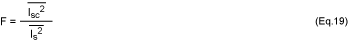
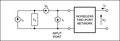
Figure 4. This noise model lets you
calculate the amplifier noise figure.
Because Isc = -Is + In +VnYs,
it follows that the mean square of Isc is given by equation 20:

Because noise from the source and noise from the two-port network are
uncorrelated:

and equation 20 reduces to:

Substituting equation 20 into equation 19 gives:
There is some correlation between external sources Vn and In.
Hence, In can be written as the sum of two terms—one uncorrelated to
Vn (Inu) and one correlated to Vn (Inc).
Thus:

Furthermore, the relation between Inc and Vn in terms of a
correlation admittance Yc is defined as:

Yc is not an actual admittance in the circuit; it is defined by
equation 25 and calculated as follows. From equation 24:

Multiplying equation 26 by Vn*, taking the mean, and observing that  : :

Substituting equation 26 into equation 23 produces the following expression for
F:

Noise produced by the source is related to the source conductance by:

where Gs = Re[Ys]. The noise voltage can be expressed in
terms of an equivalent noise resistance Rn as:

and the uncorrelated noise current can be expressed in terms of an equivalent
noise conductance Gu:

Substituting equations 29, 30, and 31 into equation 28, and letting:

and:

gives:
The noise factor can be minimized by properly selecting Ys. From
equation 34, F is decreased by selecting:

Hence, from equation 34:

The dependence of the expression in equation 34 on Gs can be
minimized by setting:

This gives:
Solving for Gs:

The values of Gs and Bs in equations 39 and 35 give the
source admittance, which results in the minimum (optimum) noise figure. This
optimum value of the source admittance is commonly denoted by Yopt =
Gopt + jBopt; that is:

From equation 36, the minimum noise figure Fmin is:

Solving equation 39 for Gu/Gopt and substituting into
equation 41 gives:
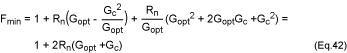
Using equation 42, equation 34 can be expressed as:

Solving equation 39 for Gu and substituting into equation 43, the
expression for F can be simplified:

Equation 44 shows that F depends on Yopt = Gopt + jBopt,
and on Fmin. When these quantities are specified, the value of noise
figure F can be determined for any source admittance Ys. This
equation can also be expressed as:

where m = Rn/Z0 is the normalized noise resistance and ys
= YsZ0 is the normalized source admittance:

yopt is the normalized value of the optimum source admittance:

Admittances ys and yopt can be expressed in terms of
reflection coefficients:
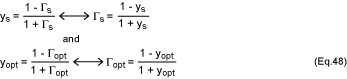
Expressing ys and yopt in terms of reflection coefficients
helps formulate the noise figure (equation 45) as a function of those
coefficients. This formulation is more convenient for industrial LNA
applications because in most data sheets, the LNA characteristics are expressed
as a table of S parameters and the optimum reflection coefficient Gopt
vs. frequency:
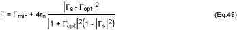
When the noise figure is expressed as a function of a circle, it can be used
with a Smith chart for optimum noise-figure matching in specific applications:
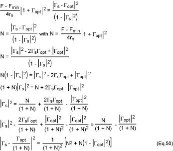
For LNA input matching, a noise circle is positioned on the Smith chart as
follows:
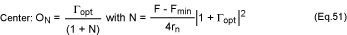
From equations 51 and 52, one can visualize the noise performance of an LNA by
plotting the noise circles on the Smith chart. This technique allows the
designer to see the effect of tuning in order to estimate the practical noise
performance.
Designing for Optimum Noise Figure
For any two-port network, the noise figure measures the
amount of noise added to a signal transmitted through the network. For any
practical circuit, the signal-to-noise ratio (SNR) at its output is worse
(smaller) than at its input. In most circuit designs, however, the noise
contribution of each two-port network can be minimized through a judicious
choice of operating point and source resistance.
The preceding section demonstrates that for each LNA (indeed, for any two-port
network), there exists an optimum noise figure. LNA manufacturers often specify
an optimum source resistance in the data sheet. As an alternative, data sheets
for the MAX2656 and other LNAs specify an optimum source-reflection coefficient.
To design an amplifier for minimum noise figure, determine (experimentally or
from the data sheet) the source resistance and bias point that produce the
minimum noise figure for that device. Then force the actual source impedance to
"look like" that optimum value with all stability considerations still applying.
If the Rollet stability factor (K) is calculated to be less than 1 (K is defined
as a figure of merit for LNA stability), then you must be careful in choosing
the source and load-reflection coefficients. For an accurate depiction of the
unstable regions, it is best to draw stability circles.
After providing the LNA with optimum source impedance, the next step is to
determine the optimum load-reflection coefficient (ΓL) needed to
properly terminate the LNA's output:

where ΓS is the source-reflection coefficient necessary for minimum
noise figure. (The asterisk in the above equation indicates the conjugate of the
complex quantity ΓL.)
Applications
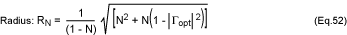
A practical example to illustrate the theory of optimum noise
matching for LNAs is the MAX2656 - an LNA (Figure 5) with high
third-order adjustable intercept point (IP3). Designed for PCS phone
applications with gain selected by logic control (14.5dB in high-gain mode and
0.8dB in low-gain mode), the amplifier exhibits an optimum noise figure of 1.9dB
(depending on the value of bias resistor RBIAS). The MAX2655/MAX2656
IP3 is adjusted with a single external bias resistor (RBIAS), which
lets you optimize the supply current for specific applications.
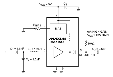
Figure 5. This typical operating circuit for the MAX2656 LNA shows
design values for the input-matching network.
Figure 5's application employs a MAX2656 LNA operating at a PCS receiver
frequency of 1960MHz and noise figure of 2dB (as requested by design). It must
operate between 50Ω terminations. As described in the MAX2656 data sheet, the
optimum bias resistance (RBIAS) for minimum noise figure is 715Ω. The
optimum source-reflection coefficient ΓOPT for minimum noise figure
in a 1960MHz application (FMIN = 1.79dB) is:

A source impedance with noise-equivalent resistance RN = 43.2336Ω
yields the minimum noise figure.
A MAX2656 LNA operating at 1960MHz has the following S parameters (expressed as
magnitude/angle):
- S11 = 0.588/-118.67°
- S21 = 4.12/149.05°
- S12 = 0.03/167.86°
- S22 = 0.275/-66.353°
The calculated stability factor (K = 2.684) indicates unconditional stability,
so we can proceed with the design. Figure 5 shows design values for the
inputmatching network. First, a Smith chart for input matching shows (in blue)
the 2dB constant-noise circle requested by design (Figure 6). For
comparison, note the dotted-line depiction of constant-noise circles
corresponding to the noise figures of 2.5dB, 3dB, and 3.5dB.
Figure 6. The solid circle on this Smith chart depicts the desired (optimum) 2dB
noise figure for a MAX2656 PCS LNA with input matching.
For convenience, we chose a source-reflection coefficient of ΓS =
0.3/150° on the 2dB constant-noise circle. The normalized 50Ω source resistance
is transformed to ΓS
using two components: the arc ΓSA (clockwise in the impedance chart)
gives the value of series inductance L1. Arc BO (clockwise in the
admittance chart) gives the value of shunt capacitor C1.
The value of arc ΓSA measured on the plot is 0.3 units, so Z = 50 x
0.3 = 15Ω. Thus, L1 = 15/ω = 15/(2πf) = 15/[2π
x (1.96 x109)] = 1.218nH, rounded to 1.2nH. The value of the arc BO
measured on the plot is 0.9 units, so 1/Y = Z = 50/0.9 = 55.55Ω. Thus, C2
= 1/(55.55 x ω) = 1/(55.55 x 2πf) = 1/[55.55 x 2π
x (1.96 x 109)] = 1.46pF, rounded to 1.5pF.
C1 is simply a high-valued DC-isolation capacitor and does not
interfere with the input matching. The chosen ΓS provides the
load-reflection coefficient needed to properly terminate the LNA:

This value and the normalized load-resistance value are plotted in Figure 7,
which also shows a possible method for transforming the 50Ω load into ΓL.
For this example, note that a single series capacitor provides the necessary
impedance transformation.
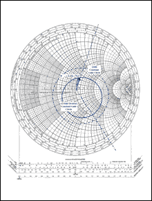
Figure 7. The MAX2656 PCS LNA has output matching for a desired (optimum) 2dB
noise figure.
The arc OΓL (counterclockwise in the impedance chart) gives the value
for series capacitor C3. The value of arc OΓL measured on
the plot is 0.45 units, so Z = 50 x 0.45 = 22.5Ω. Thus, C3 = 1/(22.5
x ω) = 1/(22.5 x 2πf) = 1/[22.5 x 2π
x (1.96 x 109)] = 3.608pF, rounded to 3.6pF.
Conclusion
These calculations have determined the matching components required for optimum
noise performance in the LNA of Figure 5. Of course, in low-cost applications
where optimum noise performance is not mandatory, C3
can be omitted, and the MAX2656 can be connected directly to a 50Ω system.
References
- Gonzalez, Guillermo; Microwave Transistor Amplifiers, Analysis & Design;
Second Edition, Prentice Hall, Upper Saddle River, New Jersey 07458.
- Bowick, Chris; RF Circuit Designs; Howard W. Sams & Co. Inc., a publishing
subsidiary of ITT.
|