ADVANCED CONCEPTS IN LARGE-SCALE NETWORK SIMULATION
David M. Nicol
Mitsuru Egashira , Takeshi Konno and Mikihiko Kobayash
Innovative Materials Engineering Laboratory, National Institute for Materials Science, Sengen 1-2-1, Tsukuba, Ibaraki 305-0047, Japan
Our probe manipulation apparatus has the ability to weld using a tungsten needle-like probe as an electrode, assisting with ease of manipulation of fine metal particles. Gold particles 60-80 um in diameter were welded to a gold substrate using the apparatus. Contact welding is carried out by applying high voltages of 4 kV or more to the probe which is in contact with the particle at a very low contact pressure. In this paper, estimation of the welding strength is done and the joint is strengthened by arcing. After welding, the joint was fractured by tensile loading, and the fractured surface was observed by SEM. The area of the joint is within a circle of 5 um in diameter regardless of welding time of 0.5-10 s. The fracture load is estimated to be about 2.6 x 10_3N. This value is 50,000 times greater than the weight of an 80-um gold particle, but is only 0.26 gf. Arcing by the apparatus, which we term ‘non-contact discharge’, appears to strengthen the joint. The probe is positioned above the welded particle and 2 kV is applied to the probe. The particle is taken off after the non-contact discharge, and the surface is observed to be fractured. Non-contact discharge was conducted in air and in N2 gas flow. Only non-contact discharge in N2 gas flow is effective for strengthening the joint. The top of the particle is sputtered by the discharge streamers. The sputtered droplets are scattered around the particle during non-contact discharge in the air but pile up near the root of the particle with N2 gas flow. The droplets form an annular ridge to which the particle becomes attached. The welding strength is, therefore, increased by non-contact discharge in N2 gas flow. © 2006 NIMS and Elsevier Ltd. All rights reserved
1. Introduction
Particle assemblage is a microstructure fabrication techni¬que that has the potential to supersede lithographic methods. The handling methods of fine particles can be classified into two types. In one, multiple particles are arranged in one step, such as by self-assembly [1,2]. In the other, fine particles are handled individually, such as by manipulation using a probe [3,4], laser [5] or microgripper [6].
The former type of method features high productivity, and has attracted considerable research interest. Photonic crystals and biosensors are fabricated this way [7,8]. The latter types of methods are being investigated mainly in relation to robotics [3] and MEMS [9,10]. Individual2. Experiments
2.1. Apparatus
system. A tungsten needle-like probe (hereinafter referred to as a probe) is positioned vertically above the worktable. Two microscopes focus on the tip of the probe and the surrounding area from different directions on the horizo¬ntal plane. The probe and the microscopes are fixed and the worktable is moved using the stage system. In this paper, however, we describe the process as if the probe moves. Pictures of the microscopes are displayed on a monitor and recorded on a video player through CCD cameras attached to the microscopes.
A DC power supply (Max-Electronics, RHV) is used to apply voltage between the probe and the substrate. The maximum output voltage is 10kV and the maximum output current is limited by a resistance to 1 mA. A stainless steel tube with an internal diameter of 8 mm is arranged concentrically around the probe and an inert gas is passed down through the tube.
The apparatus is placed in a room where the humidity and temperature are kept at 5–15% and 18–20 1C, respectively. Details of the apparatus are described in a previous paper [12] except for the inert gas flow mecha¬nism. The apparatus was used for the experiments in this study.
2.2. Welding method
Contact welding is analogous to spot welding. A particle adhered at the tip of the probe is placed on a metal substrate and high voltages of 4kV or more are applied to the probe which is held at a very low contact pressure with the particle. The particle is thus welded to the substrate
spot welding. The contact pressure must be very low to maintain the resistance between the probe and the substrate at above 100 kO. Again, in contrast to spot welding, the work pieces are pressed by the electrode and the pressure must be maintained during heating. Our method is, therefore, called contact welding.
2.3. Evaluation of welding
particle is very small. Indirect estimation from fractured area is carried out. The tip of the probe is adhered to the top of the particle, which is welded to the substrate, using a small amount of cyanoacrylate glue (Toagosei Co., Ltd., GL-10). The welded joint is fractured by pulling up the probe, and the fractured surface is observed using an SEM
The probe is a tungsten needle (NPS Inc., W26-05-01 x 1-1/2), as used for probe cards. The diameter and the point radius of the probe are 660 and 2 um, respectively. The particle is a gold sphere 60-80 um in diameter. The substrate is a gold thin plate 300 um in thickness, bonded with an adhesive agent to a 1.5mm-thick copper plate. The resistance between the copper plate and the gold plate is less than 1 Q/cm2, since high pressure is applied during adhering.
3. Results and discussion
3.1.Contact welding
A gold particle is welded to the substrate by contact welding. The probe is placed above the particle and is moved downward till it touches the particle. The power supply, set to 10 kV, is turned on and then turned off after a prescribed time
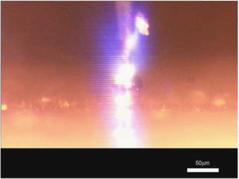
A flash of bright white light is seen immediately after the switch on, but nothing further is seen during the process. Video evidence demonstrates that the flash is generated at the contact point between the particle and the probe.

The flash is due to spark discharge caused by breakdown of the thin oxide film on the probe. No flash is observed at the contact area between the particle and the substrate. The particle is, however, welded to the substrate. Blue light is seen around the probe in Fig. 1. It is due to reflection of ordinary illumination, because it is observed before switch-on

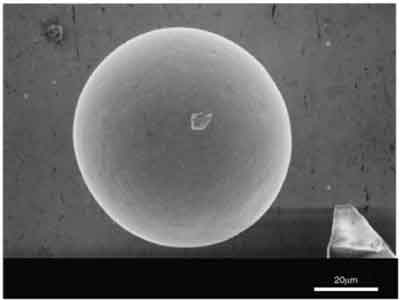
Fig. 2 shows a top view of a particle welded by the contact welding. The welding time was 2 s. The irregular mark near the center of the particle is a trace of local fusion caused by the spark discharge. Except for this trace, no other change caused by contact welding is observed on the particle or the substrate.
3.2.Evaluation of contact welding
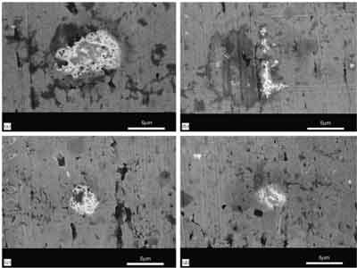
Contact welding was conducted at various welding times ranging from 0.5 to 10 s, after which the particles were detached using the method described in Section 2.3.

It may be concluded that the joint strength is not affected by the welding time. The tensile strength of gold isabout 108 MPa [14]. Assuming that the contact area is a circle of 5 um in diameter, the fracture load on the welded part is estimated to be about 2.6 x 10_3N. This value is 50,000 times greater than the weight of the 80-um gold particle.
Source of information: http://iopscience.iop.org/1468-6996/7/7/A23/pdf/1468-6996_7_7_A23.pdf