|
Introduction
As data rates in serial links push the limits of available IC processes, CDR architectures are relying on the benefits of bang-bang phase detectors (PDs) in order to achieve required performance. Specifically, bang-bang PDs can run at the highest speed a process can make a flip-flop, and suffer no systematic phase offset since data is sampled as part of the phase detector's operation. In addition, bang-bang PDs easily generalize to multiple-phase structures, allowing performance at rates where it would be impossible to construct a working flip-flop.
Traditionally bang-bang PLLs have been accused of exhibiting higher jitter than their linear counterparts. Furthermore, they suffer from finite capture range, necessitating a frequency acquisition aid in-order to lock. Increasing capture range, and also locking time, requires a larger loop gain, but this deteriorates jitter performance. Techniques to improve acquisition time have focussed on designing fast frequency acquisition aids, while freeing loop gain to control jitter characteristics. Another approach employs two discreet loop gains depending on whether the phase error magnitude detected is greater than π/2, thus improving capture range without compromising jitter performance in lock. That design required a 4-phase clock to operate.
This paper presents a bang-bang PLL scheme that dynamically adjusts its gain to achieve both fast locking and small jitter when in lock. A shift register is used to measure run lengths of consecutive UP or DN pulses, and this information is used to modulate the PLL loop gain. Results presented later demonstrate a significant reduction in acquisition time while exhibiting smaller jitter when in lock. The instance of the scheme simulated did not exhibit noteworthy improvements in capture range, but providing certain guidelines are followed, capture range can be at least as large as that of a conventional bang-bang PLL.
This paper also presents an analysis of capture range for bang-bang type PLLs. Recent works analysing bang-bang type PLLs have focussed on jitter and tracking performance when close to lock, but fail to give any insight into behaviour given a significant frequency error. The analysis presented yields a limit for pull-in range stability. This result is very important for designing frequency acquisition aids for bang-bang PLLs.
Proposed design
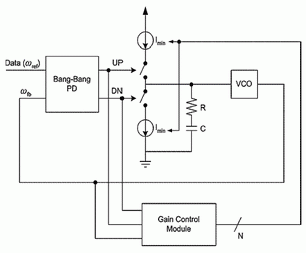
The PLL structure presented (Fig. 1) improves on the performance of a basic Bang-Bang PLL by including a module that scales loop gain depending on the distance that the PLL is from lock. When the PLL is far from lock, it is desirable to have a larger loop gain to improve locking time, and capture range. In contrast, a small loop gain is desirable when the PLL is locked so as to control jitter. The gain control module estimates how far the PLL is from lock by considering the current run length of consecutive UP or DN pulses. When a large number of consecutive UP or DN pulses occur in a row, the PLL is considered far from lock, so the gain control module outputs a large gain. In contrast, a small number of consecutive UP or DN pulses is typical of a PLL fluctuating around lock, so the loop gain is reduced. Specifically, the gain control module scales the PLL loop gain during a run of consecutive UP or DN pulses by:
 (1) (1)

Fig. 1 Proposed design scales Icp to improve dynamics
Where K is a constant greater than 1, and l is the current run length of consecutive UP or DN pulses. This method actually has a significant impact on locking time. When a PLL is acquiring lock, we expect large runs of UP pulses and shorter runs of DN pulses (if the PLL output frequency is less than the reference frequency). Thus during the longer runs of UP pulses the PLL's average loop gain is significantly grater than during the shorter runs of DN pulses. This results in dramatically reduced acquisition times, as the results presented later demonstrate.
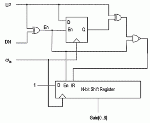
Figure 2 shows how the gain control module is implemented. The EN signal determines when a valid UP or DN signal is output. For every valid pulse (either UP or DN is asserted), the shift-register and flip-flop shown are enabled. During a run of consecutive UP pulses, the flip-flop stores а '1’, and during a run of consecutive DN pulses a '0' is stored. Every time the run type changes (found by comparing the flip-flop contents with the current pulse type), the shift-register asynchronous reset signal is asserted, clearing the shift-register contents.
Each bit of the shift register is used to enable a pair of current sources in the PLL charge pump. Each current source pair should be sized in order to approximately satisfy (1) for some k. To avoid nil charge pump current, the current source pair that would otherwise have been enabled by the first bit of the shift register is set constantly on. By ignoring the first bit of the shift register, we also avoid the charge pump current fluctuating between Imin and k*Imin, which reduces jitter when in lock.

Fig. 2 Gain control module implementation
The length of the shift register N needs to be sufficiently long to identify long runs of UP or DN pulses, without excessively adding to the PLL's complexity. If the shift register is too long though, the capture range of the PLL can be reduced. The results presented in the following sections assume an 8-bit register, and k= 1.32 which allows the PLL loop gain current to be scaled by a factor of approximately 1 to 9.
The logic comprising the dynamic gain control module is simple; the critical path consists of an AND gate and an XOR gate. Thus the speed advantages of using a bang-bang phase detector are not lost.
Design performace
This system was modelled first in Matlab-Simulink, then implemented at the transistor level and simulated in SPICE. To evaluate performance, a reference design was also simulated in Matlab-Simulink and SPICE.
The Simulink designs employed ideal models for current sources, switches, digital circuits, and the PLL VCOs. The reference PLL design was implemented with a fixed loop gain kref, and the PLL with dynamic gain control was configured with a loop gain spanning  to 3 * kref. to 3 * kref.
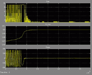
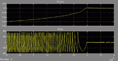
Figures 3 and 4 compare the phase error and average VCO control voltage Vc_ave (the voltage across the loop filter capacitor) of the new design with the reference design during acquisition. In this example, the initial frequency error is set to 6% of the reference frequency (close to the pull in limit). As can be seen, during frequency acquisition, the gain of the new design is high leading to more than 50% reduction in locking time. Jitter measurements in lock show that the peak to peak jitter of the new design is almost one third that of the reference design, which is what we predict.

Fig. 3 Dynamics of bang-bang PLL with dynamic gain control during aquisition

Fig. 4 Dynamics of reference bang-bang PLL during aquisition
Summary and Conclusions
This paper presents a novel bang-bang PLL scheme that improves locking time, without sacrificing jitter performance when in lock. It achieves this by dynamically scaling the PLL loop gain depending on how far the PLL is from lock. The digital circuitry used to implement the gain control unit consists of a shift register, and no more than two levels of logic; thus the PLL can run at close to the speed of a flip flop. Providing the gain control module is carefully designed, capture range for the PLL can be at least as large as that of a conventional PLL. To ensure capture range is not negatively impacted by the gain control module, the average loop gain of the PLL at the pull in frequency should be checked.
The design was examined first via behavioural simulation in Matlab Simulink, then by physical simulation. The results obtained demonstrate significant improvements to acquisition time and jitter performance.
|
