Time-to-Voltage Converter for On-Chip Jitter Measurement
by: Tian Xia, Member, IEEE, and Jien-Chung Lo, Senior Member, IEEE
Source: http://www.emba.uvm.edu/~xiat/papers/tim03.pdf
In this paper, we present the concept and design of a time-to-voltage converter (TVC), and demonstrate its application to on-chip phase-locked loop (PLL) jitter measurement. The TVC operates in an analog, continuous mode without using a sampling clock. It compares the signal under measurement with a reference signal by charging and discharging a capacitor. First, the low-frequency reference signal charges the capacitor in one cycle. Then, the jitter signal discharges the same capacitor repeatedly until the voltage on the capacitor falls below a threshold. The number of times the jitter signal needs to discharge the capacitor is recorded on a binary counter. We demonstrated that a 160-ps injected jitter is successfully measured by the proposed TVC with a 2-MHz reference signal. An 8% measurement error is found in experiment, using four-bit counters.
Charge pump, on-chip measurement, phaselocked loop (PLL), signal jitter, time-to-voltage conversion (TVC).
N THE 2001 edition of the International Technology
Roadmap for Semiconductor [1], timing jitter measurement
in high-speed VLSI is stated as one of the top most difficult
challenges. In this paper, we propose the
concept of time-to-voltage converter (TVC) circuit. Specifically, the TVC operates directly with the analog voltage
level that represents the timing values. The measurement
circuit is thus compact enough to be implemented on the chip.
This, in turn, reduces the possibility of environmental noise
interference.
Timing measurement is an important part of many applications
such as laser radar, phase meter, PM or FM demodulators,
etc. [2]–[4]. In particular, a class of time-to-digital converter
(TDC) has been developed for these applications. Similar idea
has never been considered for testing deep sub-micron VLSI
to our best knowledge. The proposed TVC is a modified form
of TDC such that the timing information is transformed to
voltage level directly without digitization [5].
Figure 1. shows the proposed on-chip jitter measurement circuit for a PLL based frequency synthesizer. The jitter measurement circuit is composed of a charge pump, an XOR gate, an analog comparator with hysteresis, a capacitor, and a digital counter.

We can see that the test circuit does not directly
measure signal SVCO, it uses the input jitter free signal Sref to
measure the feedback signal Sz. For a PLL, its PFD compares
two input signals Sref and Sz, and generates two output signals
U and D. If Sref’s phase is ahead of Sz’s, there will be a pulse in
U. Similarly, if ’s phase falls behind of ’s, the pulse will
appear in D. The pulse width is proportional to the phase error.
Therefore if we can measure the pulse width of U and/or D, we
will be able to calculate the timing jitter in Sz .
In the charge pump, Sref and Vcmp control switches S1 and
S2, respectively, while the jitter pulse Vj and and D flip-flop’s
output Vncmp control S3 and S4 separately. Capacitor Cp connects
to analog comparator’s negative input pin. The voltage
source Vcent decides the central voltage of the comparator’s
hysteresis, while Vbase sets the base voltage for the capacitor Cp. Their values are set to be
Vcent=2.5 v, and Vbase=2.3 v. Actually, Vbase equals comparator’s threshold voltage VIL.
Thus, during measurement, the charging or discharging
process will start from or stop at this voltage point.
When the measurement process starts, since VIIN is less than Vcent
initially, comparator’s output Vcp is high, and D flipflop’s
output Vcmp is high too. So, switch S2 is on. In Sref’s
positive half cycle, switch S1 is conducted. Thus the capacitor Cp
is charged with current source Ic. When the voltage on comparator’s
inverse input pin reaches or becomes higher than the
threshold voltage VIH, Vcpwill be toggled to logic-0. When a
new rising edge of Sref comes, the D flip-flop’s output Vcmp
flips to low and Vncmp flips to high. Thus switch S2 is cut off,
and the charging process stops. By setting the Ic amplitude and Cp
size, we can control the charging process to finish in one Sref cycle.

At the end of the charging process, Vcmp is high, S4 is conducted,
so the discharging process is enabled. Simultaneously,
a digital counter is activated to count the number of clock cycle
of Sref during discharging process. When there are jitter pulses
coming from the output of phase/frequency detector, switch S3
is conducted and the capacitor Cp is discharged by current sink Id,
the voltage over the capacitor is then decreased. When the
voltage over the capacitor drops back to will flip to VIL, Vncmp
logic-1, S4 is then cut off. The discharging process is thus ended.
At this moment, the datum Nc at the binary counter’s output is
locked and read out. Using this number Nc , we can calculate the
jitter value in Sz.
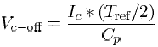
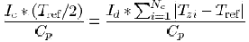
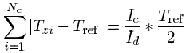
Since the Sref’s duty cycle is 50%, its positive pulse width is Tref/2. The charging voltage offset is
The discharging voltage offset is
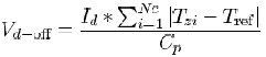
Because these two voltage offsets are controlled to be equal during the measurement process, we have Vd-off=Vc-off, so
Thus
The average jitter amplitude Jz is
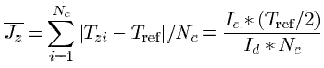
From the above equations, we can see that the jitter amplitude
could be calculated by the discharging and charging current
ratio Id/Ic, the period of the reference clock signal Tref,
and the counter’s output value Nc. Id/Ic ratio is known before
the measurement, which is decided by the sizes of transistors
in the current mirror, and Tref is also a pre-known parameter.
Therefore, the only number we need to measure is Nc.
Here, a 160-ps jitter signal has been injected into the PFD’s
output for the simulations. In Fig. 10, we show the HSPICE simulation
results. The first signal shown at the top is the input reference
signal Sref with 2-MHz frequency. The second waveform
is the injected jitter signal with a pulse width of 160 ps. The
third one is the voltage fluctuations over the capacitor Cp. We
can see, it takes 1 Sref cycle to finish the charging process. The
fourth and the fifth waveforms are signals Vcmp and Vncmp ,
which are the outputs of the D-flip flop. The last four signals
represent counter’s outputs Q3, Q2, Q1 and Q0, respectively.
Their values represent the number of cycles of the discharging
process. In this case, Ic=3.24 mA and Id=4.62 mA.
At the end of the simulation, when Vcmp=1, we obtain Nc=(1100)2. According to (16), we find
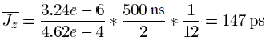
So, the measured jitter is 147 ps while the injected jitter is 160 ps. The measurement error is about 8%.
To design an on-chip measurement circuit, several factors
need to be considered, measurement time, measurement resolution,
the effect of process variations in fabrication, and
resource overhead. According to the above analysis, we know
the measurement time length is (1+Nc)*Tref,
is the time length of the discharging process 1*Tref is the
time length of the discharging process.
Thus, to shorten the measurement time, we should try to make Ncsmaller. From
Figure 3, we can see, when the jitter is within some certain
range, the value of Nc is inversely proportional to the current
ratio of Id/Ic, which means by increasing the current ratio of Id/Ic,
we can make Nc small, and expedite the measurement
process. However, Id/Ic ratio cannot be increased limitlessly,
because its value also decides the measurement resolution.

In Figure 15, we show the layout of the PLL and the proposed built-in jitter measurement circuit. The large area in the lower right hand corner of the proposed measurement circuit is the capacitor Cp. Based on this layout, the area overhead of the proposed design is about 21%. We remark here that the overhead ratio sounds high because of the small size of PLL. The proposed design is quite compact.

We have presented a design of TVC and demonstrated its application to the on-chip jitter measurement in the PLL-based frequency synthesizer. By charging and discharging on the same capacitor, we cancel out the need to have a precise capacitor be fabricated (which is almost impossible). This is crucial for on-chip measurement as it eliminates the tedious tuning process. Further, the TVC takes timing measurement without a sampling clock. Note that the sampling clock in the conventional approach must be an order of magnitude faster than the signal to be measured. In the demonstrations above, the Sref is an order of magnitude slower than the jitter under measurement.
[1] International Technology Roadmap for Semiconductors [Online]. Available: http://public.itrs.net/Files/2001ITRS/Home.htm
[2] A. Rothermel and F. Dell’ova, “Analog phase measuring circuit for digital CMOS ICs,” IEEE J. Solid-State Circuits, vol. 28, pp. 53–856, July 1993.
[3] P. Chen and S.-I. Liu, “A cyclic CMOS time-to-digital converter with deep sub-nanosecond resolution,” in IEEE Custom IC Conf., 1999, pp. 605–608.
[4] E. Raisanen-Ruotsalainen, T. Rahkonen, and J. Kostamovara, “An integrated time-to-digital converter with 30-ps single-shot precision,” IEEE J. Solid-State Circuits, vol. 35, pp. 1507–1510, Oct. 2000.