PLL On-Chip Jitter Measurement: Analysis and Design
Carl W. Werner, Don Draper, Borivoje Nikoli
Analysis of on-chip jitter measurements based on the dead-zone method reveals potentially large errors in the jitter variance estimate, when the jitter distribution is changing or not known a priori. To overcome this, a more accurate variance estimation method is proposed and experimentally verified. The residual error, caused by the correlated noise between the PLL and the measurement circuit, is fully characterized and circuit topologies are proposed to mitigate this type of error.
On-chip jitter measurement has been proposed to adaptively
optimize the PLL performance [1,2]. This paper studies the
limitations of on-chip jitter measurement based on the deadzone
method and improves on it by proposing a new jitter
metric.
Fig. 1a shows the jitter measurement circuit based on the
dead-zone method [3]. The phase of the PLL output clock is
compared to that of the delayed reference clock фREF. The
control voltage of the delay line (VCDL) is adjusted so that the
фREF phase converges to the specified tails of the jitter
distribution. The dead zone width is assumed to be a measure of
the RMS jitter, Fig. 1b. The tunable PLL uses a dual-chargepump,
self-biased architecture [4] with charge pump currents
that are controlled by 4-bit DACs. The damping factor is
proportional to the current ICP2. For low values of ICP2, the
damping factor decreases causing peaking of the noise transfer
function and increase of the PLL jitter. For high values of ICP2,
the PLL jitter increases again due to increased phase detector
frequency spurs and/or lower phase margin. The minimum jitter
corresponds to intermediate values of ICP2..

The RMS jitter estimate based on the dead-zone
measurement method may be inaccurate, if the jitter distribution
shape varies at different operating points. Furthermore, various
noise sources induce jitter both in the PLL and the
measurement circuit, and this noise correlation may affect the
measurements.
To study the performance of the jitter measurement
procedure, the PLL and the jitter measurement circuit were
implemented in a 0.13 мm CMOS process, Fig. 2. At 1 GHz,
the PLL and measurement circuits consume 17mW and 10mW,
respectively. Power consumption of the measurement circuit is
less important, as it can be powered down after it determines
the optimal PLL operating point. A delay line is used to align
the PLL output clock with the reference phase фREF at the
beginning of each experiment, in order to increase the dynamic
range of the measurements. The same effect is achieved by
increasing the length of the VCDL in the measurement circuit.
The jitter estimation algorithm was implemented in software for
added flexibility. A digital oscilloscope is used to verify the
accuracy of the on-chip measurements.

Fig. 3 shows the measured variance of the PLL jitter at various damping factors while operating at 1GHz along with jitter histograms from scope measurements. At high damping factors the jitter distribution changes to bimodal Gaussian due to the periodic jitter from the phase detector spur. As the distribution deviates from Gaussian, the error due to the deadzone method increases. This indicates that the minimum jitter could be correctly identified from on-chip jitter estimates, if the variance could be calculated more accurately from arbitrary jitter histograms.

To combat the dead-zone errors, a new jitter variance metric (VM) is proposed, which makes no assumption about the shape of the jitter distribution:
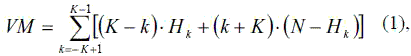
where Hk is the cumulative number of hits at position k, N is the number of edges compared during a measurement, and 2K-1 is the number of histogram partitions, Fig. 4a. Fig. 4b shows the VM calculations for the histograms of Fig. 3. If the histogram partition width dx is small enough, the shape of the VM curve follows that of the measured jitter curve. The proposed algorithm utilizes the simple hardware of Fig. 1a, and its implementation does not require multiplication, as shown in the simplified schematic of Fig. 5. The histogram partition counter controls the DAC, which determines the phase фREF. The control logic ensures that the term Hk (N-Hk) is added K-k (k+K) times during the VM calculation, see Eq. (1), where k is the histogram partition index.


After compensating for the dead-zone error, the residual error is due to correlated noise between the PLL and the measurement circuit. The on-chip measurement estimates the jitter of the phase difference between the two clocks at the input of the phase arbiter:

The correlation term - 2*Cov[фPLL, фREF], caused both by
supply/substrate noise and reference clock jitter, depends on the
PLL operating point, and may affect the jitter estimates.
The variation of the correlation errors across the PLL
operating points is relatively small, Fig. 6. The correlation
errors due to supply noise affect the relative jitter values more
than the ones due to refclk jitter. Almost all of the supply
correlation error is produced by the interaction of the supply
noise spectrum spur at the refclk frequency, Fig. 7a, with the
component of the PLL phase detector spur due to supply noise,
Fig. 7b. It can be shown that this main component of the supply
correlation error can be removed by eliminating the alignment
delay line.
Thus, with adequate jitter metric and appropriate circuit
topology, very accurate on-chip jitter measurements can be
performed and used for PLL adaptation.


The work of S. Vamvakos and B. Nikoli was supported in part by MARCO C2S2. The authors would like to thank R. Kollipara and A. Tonizzo of Rambus, Inc. for technical support.
[1] M. Mansouri et al., “Methodology for On-Chip Adaptive Jitter
Minimization in Phase-Locked Loops,” IEEE Trans. Circuits Syst. II,
vol. 50, no. 11, pp. 870-878, Nov. 2003.
[2] S. Vamvakos et al., “PLL Architecture for Adaptive Jitter
Optimization,” Proc. ISCAS, vol. IV, pp. 161 – 164, May 2004.
[3] Y. Moon et al., “A 0.6-2.5 Gbaud CMOS Tracked 3x
Oversampling Transceiver with Dead-Zone Phase Detection for
Robust Clock/Data Recovery,” IEEE J. Solid-State Circuits, vol. 36,
no. 12, pp. 1974-1983, Dec. 2001.
[4] J. G. Maneatis, “Low-Jitter Process-Independent DLL and PLL
Based on Self-Biased Techniques,” IEEE J. Solid-State Circuits, vol.
31, no. 11, pp. 1723-1732, Nov. 1996.