Kevin A. Kwiat, Ph.D., Air Force Research Laboratory (AFRL/IFGA)
For over a quarter of a century now an eon in the course of development of modern computers the tenet that hardware and software are logically equivalent has remained unchanged [1], [2]. This tenet has not only withstood change, it has become the basis for a vibrant approach to computer architecture: reconfigurable computing. Choosing whether or not to implement logic in hardware or software has always been a design decision based on where to migrate the complexity: to hardware or software. High speed usually means a hardware-intensive implementation whereas a way to reduce the size, weight and power (SWAP) of hardware is to rely more on a software-intensive implementation. The 1990's saw the distinction between hardware and software blurred by static-RAM (SRAM) based Field Programmable Gate Arrays (FPGAs): with every new data loaded into their on-chip configuration memories, these FPGAs realized a new hardware function. The contents of configuration memory became the software that changes into hardware. Now algorithms that previously, due to their complexity, could only be realistically considered for software implementations have a feasible path to a direct hardware implementation. Accepting of this migration from software to hardware are SRAM-based FPGAs. Those SRAM-based FPGAs that permit writing and rewriting portions of their configuration memory concurrent with device operation are called dynamically reconfigurable FPGAs. With the ability to change software into hardware on the granularity of individual logic gates, dynamically reconfigurable FPGAs go the furthest towards making hardware appear like software. Designers have manipulated the flexibility of dynamically reconfigurable FPGAs to construct reconfigurable computers [3] that offer enhanced performance while still remaining within reasonable SWAP measures. However, might the reliability of dynamically reconfigurable FPGAs, as opposed to their traditional, fixed-hardware counterparts, be their downfall?
In digital logic, the unit of measuring complexity is gates. Gates are physical entities that occupy die space, consume power and take up a chip's routing resources, so, in general, if the gate count is higher, then the reliability is lower. However, consider the notion of virtual gates: we see them but they are not there. These gates (note bold italics) are virtual in the same sense as computer virtual memory - where main memory is made to look larger than it physically is. When pages of main memory are not needed they are swapped out to disk and stored there until they are needed again. A dynamically reconfigurable FPGA's cells implement gates that are connected to form a logical function; yet when this logical function is no longer needed and the cells are being reused by another logical function, where do the gates of the previous function go? This is the key question in migrating a reconfigurable computer's complexity in a reliability-conscious way.
To answer this question, one can extrapolate from a widely accepted reliability-prediction method [4] that calculates the failure rate based on gate-count. You can then calculate the failure rate for the two cases: a conventional approach with fixed hardware logic where traditional gates are used, and the dynamically reconfigurable FPGA approach that uses gates.
For these two cases the failure rate, λ , is calculated by the formula:
| λ = (C1πT + C2πE)πQπL |
|
| where, | |
| C1 = die complexity failure rate | |
| πT = temperature factor | |
| C2 = package complexity failure rate | |
| πE = environmental factor | |
| πQ = quality factor | |
| πL = learning factor | |
In the preceding calculations, the following values are constant: πT = 0.16, πE = 0.5, πQ = 3, and πL = 1. Regarding the constant learning factor for both cases, one can use the dynamically reconfigurable FPGAs of Atmel's AT6000 series that the company advertises as mature technology (see http://www.atmel.com/products/FPGA/). Also, some early work was carried out with developing CAE tools that simulated the FPGA's dynamic reconfiguration [5]. This too contributed to a climbing of the learning curve in using gates instead of gates.
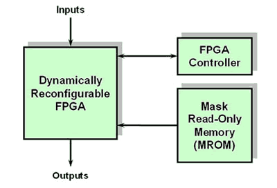
For the fixed hardware design, C1 is measured by counting the gates. Since the on-chip SRAM of dynamically reconfigurable FPGAs is volatile, external, non-volatile memory is needed to store the FPGAs configuration data. The FPGA is considered programmed when the configuration data is read from the external memory and loaded into the FPGA's on-chip, SRAM configuration memory. Therefore, only when external storage (see Figure 1) is added can the FPGA implement usable gates. The C1 for the unprogrammed FPGA is based solely on the FPGA's gate count. It is comprised of the FPGA's cells, on-chip configuration memory and internal programming logic.

Figure 1. Basic Reconfigurable Computing System
Adding external memory to store the various FPGA configurations increases the C1 factor of the reconfigurable design. However, the external memory permits us to migrate complexity from gates to gates. For external memory one can turn to a masked-programmed ROM (MROM). Typical densities of MROMs are 16 Megabits per chip. In the modeling of the AT6000, three bytes program a cell, and it is assumed that a single gate is implemented per cell. Increases in the gate count of the target design imply a 3-byte increase in the MROM on a per gate basis. For example, 1 Mbits of MROM can be used to implement 41,600 gates. The C1 value for a MROM of this size is only 0.0052, while the C1 value for the equivalent number of hardware gates is 0.29 a factor of 55 increase in complexity. With 16 Megabits of MROM, the FPGA can implement 666,666 gates.
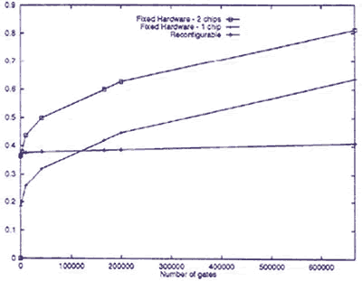
For the fixed hardware solution, consider two sub-cases. The first is a single package solution and the second is a two-package solution. The failure rate calculation for the reconfigurable approach includes three packages: the FPGA, the controller, and the MROM. The number of pins for the FPGA package is 224. The controller is assigned 1,000 gates and an initial package pin count of 36. Initially, the MROM of byte size 3 (for 1 gate) is assigned a 16-pin package. The number of address pins for the counter and the MROM are then increased with the size of the MROM needed to accommodate the gate count of the target design. Figure 2 shows the failure rates between a fixed hardware design and a reconfigurable design.
The horizontal axis is the number of logic gates required. For the fixed hardware case, this number is the same as counting the number of gates directly. For the FPGA, this is the number of gates implemented through dynamic reconfiguration where the unused gated are stored externally in the MROM. Initially, the failure rate for the unprogrammed FPGA is high due to its non-virtual gate count of 55,296. However, the complexity for each FPGA-implemented gate is placed into a significantly less complex 24-bit increment of MROM. As a result, the failure rate for the FPGA, counter and MROM grows only slightly as compared to the curves for the fixed hardware solutions. Comparing the failure rates of the reconfigurable and fixed designs, the sub-case of the single package fixed-gate solution has greater failure rates when gate counts go above 130,000. At higher gate counts, the two-package sub-case would probably occur, and as shown in Figure 2, its corresponding failure rate is dramatically greater than that of the reconfigurable design.

Figure 2. Number of Gates vs. Failure Rate (Click to Zoom)
Fixed gates of a custom application-specific integrated circuit (ASIC) could implement computer algorithms directly in hardware; yet a large number of fixed gates would be necessary. Fixed gates may be used to implement a microprocessor that runs software versions of these algorithms; however, modern microprocessors easily exceed the gate counts shown in Figure 2. Furthermore, the failure rates shown in Figure 2 do not include the memory that is required by software-based implementations of computer algorithms. Typically, microprocessor execution of the software is possible only when cache chips and memory management units augment the processor's basic CPU functions thus a multiple package solution would be expected. Driving up gate counts even more would be the need to match a reconfigured computer's ability to provide an increase in the variety of the algorithms.
Migrating computer algorithms from software to hardware and meeting SWAP requirements is not as daunting a complexity problem because of the maturing of dynamically reconfigurable FPGAs. The storing of virtual gates in mature MROM places a reconfigurable computer on a solid foundation. Solid, here, has dual meaning: in the context of reliability attributed to low device failure rate and in the context of permanence once installed in the system, changing MROM entails the prohibitive expense and toil of actual chip replacement. Although this article has demonstrated that logic gate virtualization within MROM shows promise for managing a reconfigurable computer's hardware complexity, a question arises: will the software that designers migrate to hardware be reliable enough to have them commit it to unchangeable MROM? A reliability engineer will likely be sought out for the answer.