Pipelined Multipliers and FPGA Architecture
Mathew Wojko
Dept. of Electrical and Computer Engineering
University of Newcastle
Callaghan, NSW 2308, Australia
Abstract. This paper studies pipelined multiplication techniques for implementation on FPGAs with emphasis on the utilization of FPGA hardware resource. Performance of multiplier implementations are measured for commercially available FPGA architectures where two inherent issues are introduced and investigated. These being the imbalance of critical interconnects delay between general routing and static carry interconnects and the amount of FPGA logic area used and its poor utilization. For each of these issues suggestions are proposed and investigated.
Multiplication on FPGAs is considered an expensive operation. For high throughput multiplier implementations where the result is calculated in a pipelined parallel fashion, large Logic Cell (LC) counts are required. The advent of fast-carry logic has allowed multiplier implementations to achieve sustainable speeds for many DSP operations. However for increasing bit size multiplication operations, high LC counts still provide poor FPGA device utilization limiting FPGAs from a wider range of DSP or arithmetic intensive applications.
Several techniques have been proposed to provide better utilization of the FPGA resources when implementing multiplication. Mintzer [6] noted that for fixed coefficient multiplication, by using distributed arithmetic and storing coefficient look-up information in the Look-Up Table (LUT) element of LCs within the FPGA, reduced logic implementations were achieved. Run-Time Reconfiguration (RTR) has been employed to update the content of LUTs to provide a new multiplicand value. Previous work has shown reconfigurable multiplier implementations on the XC6200 series FPGA [7,1]. Reconfiguration of LUT content is performed through the SRAM configuration interface using pre-computed configuration data. A novel approach named the Self-Configurable multiplication technique was presented by the author and ElGindy [10] for the Xilinx XC4000 series by performing the LUT reconfiguration on chip. On new input, the configuration data is computed on chip and stored into the LUTs in parallel. Other work to improve hardware efficiency for multiplier implementations suggests embedding arithmetic specific Flexible Array Blocks (FABs) capable of implementing a 4 x 4 bit multiplier, within a conventional FPGA structure [2].
However, each of these techniques results in a compromise. For the fixed coefficient technique, coefficient values cannot be updated. Reconfiguration of stored values requires additional time where the circuit is typically off-line while configuration takes place. Furthermore, for an FPGA with multiple logic cell types, segmentation in hardware utilization between the cell types occurs. This paper presents two alternatives for performing multiplication on FPGA architectures.
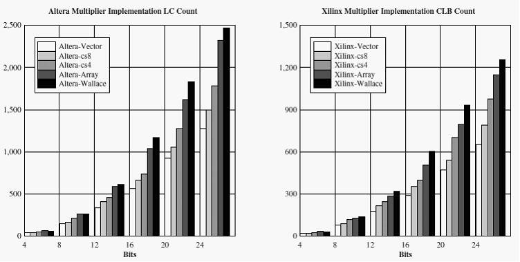
In this section we review the pipeline performance of three multiplication techniques implemented on the Xilinx XC4036EX-2 [5] and ALTERA EPF10K70RC-2 [8] devices. The parallel array, parallel add (vector based) multiplier and the Wallace carry-save multiplier are reviewed (refer to [3,9,4] for a description of the techniques). For the implementations, all techniques were pipelined at every stage of computation to achieve the highest throughput possible. Designs were targeted at the physical level, such that where possible specific architectural features (such as static carry) were utilized. Design mappings were placed and routed with high emphasis on reducing interconnects delays between successive pipeline stages. Figure 1 below compares the LC count requirements for each technique on each device while Figure 2 compares the maximum clocking speeds achieved.

Fig. 1. Multiplier implementation LC Count for Xilinx and Altera Devices.
Comparing the LC counts for each FPGA, we see the same general trend across each architecture for each technique, i.e. the logic requirements scale quadratically with the input bit size of the multiplier. We can observe the relative differences of how each technique maps to an FPGA architecture containing 4-input LUTs and static carry. The Wallace technique saves carry values from propagating within pipeline stages at the expense of additional logic, the vector and array techniques propagate carry the bit length of the input operands making use of the static carry interconnect. The parallel array technique can be viewed to require additional cells for pipeline buffering.
However, the trends observed for the maximum cycle speed for each technique in Figure 2 are different between FPGAs. This result is due to the difference in interconnecting strategies employed in both architectures. Xilinx utilizes a hierarchical scheme in which interconnect paths vary in CLB span lengths; while the Altera architecture uses row and column interconnects that span the whole device. For Xilinx, Wallace implementation results are seen to converge with vector and array for increasing input bit sizes. For Altera there is a distinct difference between them. This is because the vector and array based techniques make high use of the static carry interconnect, thus reducing the routing demand placed on the general purpose interconnect. Since the Wallace technique does not propagate any carry values, it makes no use of the carry interconnect and thus places a higher demand on the general routing interconnects. Results show that the Altera architecture is able to sustain more consistent routing delays for increasing bit input sizes through the use of spanning interconnects than the Xilinx hierarchical length interconnect architecture. This has been verified by analysis of routing floor-plans produced by the routing tools used. As routing channels become congested, determining alternate paths to establish routes requires more effort for the Xilinx interconnect than Altera.

Fig. 2. Multiplier implementation delay for Xilinx and Altera Devices
The Carry Save/Propagate (CSP) multiplication technique was developed as a hybrid between pipelined vector and carry save multiplication techniques to provide a configurable balance between LC counts, maximum clocking frequency and interconnect type utilization (i.e. static carry and general purpose). By making the carry propagation length within the multiplier a design parameter, the CSP technique establishes a continuum of multiplier instances and implementation results between the extreme cases of parallel add vector based and Wallace multiplication techniques.

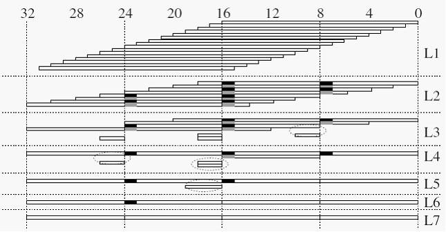
Fig. 3. 16-bit CSP multiplier example with an 8-bit carry propagation length.
In Figure 3 an example of the bit operations within a 16-bit CSP multiplier of propagation length 8 is shown. The initial array of partial products is shown at the first level (L1). These are then added in parallel to produce n/2=8 results producing 16 carry values at the 8-bit wide defined boundaries. The CSP technique maintains carry values in two ways. At each level they are registered as either a carry-in for the next stage of addition, or to be accumulated with other carry values for later addition to the partial product values (denoted respectively as black or grey). Two sets of values progress throughout the operation of the CSP multiplier, these being the accumulated values of the partial products, and the accumulated carry-save values. Add operations are performed in each set to reduce the number of values. At certain stages, additions using accumulated carry values occur (denoted by the dotted oval). The addition operations continue until the height of the array of values is reduced to one and no carry values remain as in L7.
CSP multiplier implementations were performed with the carry propagates parameter set both to 4 and 8 bits on both FPGA architectures. Results for the LC count and resulting maximum clocking frequency can be viewed in Figures 1 and 2 respectively. For increasing carry propagate length, the LC count is reduced as is the clocking frequency. In Figure 4 the utilization function is graphed on a log scale for each multiplication technique against each FPGA architecture. For the CSP multiplier, the Altera architecture appears able to leverage logic requirements by balancing the use of the static carry interconnect and general purpose routing. Thus providing higher device utilization, i.e. the shorter the carry propagation length, the higher the LC count and the higher the clocking frequency. The Xilinx architecture shows an utilization increase, but not one significant enough to show an effective balance between the use of interconnect types for the required LC count.

Fig. 4. Multiplier implementation delay for Xilinx and Altera Devices.
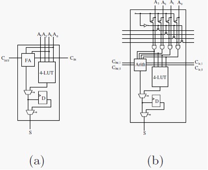
Most parallel multiplication techniques consist of two phases of operation; a partial product array is first computed, and is then reduced (typically) in parallel to provide the multiplication result. Considering how a multiplication technique maps to either the Xilinx or Altera FPGA architectures, there are two examples of poor utilization. In the generic 4-bit input LC schematic in Figure 5(a), the LC contains a 4-bit input LUT, fast static interconnected arithmetic logic and a register. This gives a typical description of the LC functionality present in both the Altera FLEX10k and Xilinx XC4000 architectures. For the first phase of multiplication, (the bit-cyclic convolution) for an n-bit multiplier n2 2-bit AND operations are performed. This requires n2 LCs to calculate the partial product array. Implementing a 2-bit AND operation on a 4-bit input LC provides extremely poor utilization of the cell. For the second phase, the partial product results are reduced by parallel addition. Pairs of values are added together to reduce the number of partial products by half between successive stages. Again, we see that each LC implements a Full Adder (FA) which again only utilizes two of the four inputs of the LC plus the static carry interconnect. It is evident that the potential bandwidth of the LC within an FPGA is not exploited and is only at half of its capacity. Due to this fact, high LC counts are required for multiplier implementations, providing poor resource utilization.
Figure 5(b) shows the suggested LC architecture that ensures the potential bandwidth of each LC is fully utilized such that reduced LC count multiplier implementations can be achieved. Added to the LC are four static interconnects with pass transistors and AND gates, and an enhanced arithmetic unit accepting four bit inputs, two carry-in values and producing a single bit result and two carry-out values. All static fixed interconnects are intended exist between rows (or columns) of LCs and not to be considered as general inputs to the LCs. For multiplier implementations, the first phase of partial product values is

Fig. 5. Common and suggested Logic Cell architectures.
computed by utilizing the top four static busses. Inputs to the LC are either be routed onto the static bus, or propagated through the ANDs gate as input to the LUT (by configuring pass transistors in the cell). This mechanism provides the ANDing phase for the multiply operation where four bit values can be broadcast to a row of LCs such that a set of 4 n-bit wide partial products can be generated internally within one row of LCs. These values can be added to provide a 4 x n multiplication result. The addition is performed by the ARITH unit shown in the figure. The unit accepts four bit values which it adds to a 2-bit carry input and produces a 3-bit output. Bit zero is output as the bit result for the cell while bits two and three are propagated to the next cell as carry-in bits. A carry-chain requiring two bits is established to add the four n-bit values within a single row of LCs. As a result, to implement a 4 x n bit multiplier using the modified LC architecture, n + 5 LCs are required. On average an n x n bit multiplier can be implemented with LC counts four times less than conventional FPGAs by using this modified LC. While it is acknowledged the Xilinx Vertex architecture enables partial product values to be generated within cells by the use of an additional AND gate, halving LC counts for multiplier implementations. The use of single bit carry lines does not allow as high utilization as the modified LC cell does.
To evaluate the effectiveness of the modified LC, the suggested changes are integrated into both the Altera and Xilinx devices and are compared with a previous study [2] on multiplier implementations. In this study, multiplier implementations using FABs are compared against those on both the Xilinx 4000 and Altera FLEX architectures. Results are presented comparing transistor counts and relative counts per bit2 for multiplier implementations on each. These results are reproduced below in Table 1 where new results are presented for the modified LC changes integrated into the FLEX and XC4000 architectures implementing vector based multipliers. Viewing the results, we can see respective improvements of factors 3.79 and 3.91 transistors per bit for the Altera and Xilinx architectures using the modified cell suggestion. While these results do not achieve the den sity provided by using FABs, they do illustrate a minor architectural change that can be made to existing FPGAs to improve multiplier implementation efficiency while not disrupting the existing architectural framework of the FPGA.
|
Implementation |
Trans. Per Cell |
Cells per Bit2 |
Trans. per Bit2 |
Relative Area |
|
FABs |
2300 |
0.0625 |
144 |
1 |
|
Altera 10k |
12000 |
0.26 |
3169 |
22 |
|
Xilinx 4000 |
3400 |
1.14 |
3880 |
27 |
|
Altera 10k Modified |
12600 |
0.066 |
832 |
5.8 |
|
Xilinx 4000 Modified |
3550 |
0.28 |
944 |
6.9 |
Table 1. Relative bit area requirement comparison.
10. M. Wojko and H. ElGindy. Self configurable binary multipliers for LUT addressable FPGAs. In Tam Shardi, editor, Proceedings of PART’98, Newcastle, New South Wales, Australia, September 1998. Springer. 347