Introduction
Currently, there is a rapid development of computer-aided design (CAD) systems. The main task of CAD is to simplify and improve the efficiency of engineers by interacting with computers. CAD is used for carrying out various technical works, facilitating design processes in various industries, improving the quality of design results, end-to-end computer-aided design, and more.
One of the main tasks of the synthesis of structures is the task of placing the elements of the switching circuit on a given switching field. The placement of elements is the task of determining their location on the switching field in a constructive module such that the best conditions are created for solving the subsequent task of tracing connections, taking into account design and technological requirements and limitations. Among the existing placement algorithms, a group of sequential algorithms most closely mimics the actions of a design engineer, while calculating a local optimality criterion.
Research objective
The goal is to develop an educational computer subsystem for the placement of a printed circuit board using the method of branches and boundaries. The placement of printed circuit boards is an important step in the design of printed circuit boards. The successful execution of the subsequent design stage depends on the quality of this stage, namely, tracing of printed connections and layering of the printed circuit board.
The concept of the computer-aided design system itself
This system (CAD) is understood as an organizational and technical system consisting of a set of design automation tools and a team of specialists from design organization departments capable of solving design problems [1]. At the moment there are several popular CAD systems, each of them has its own features and capabilities.
Currently, the main means of automation is a combination of computer technology and computational methods. There are two main groups of tasks involving the use of these tools.
The first group is related to the improvement of design methods based on mathematical modeling and automation of the search for solutions. At this level, the following is provided:
-automation of synthesis of design solutions;
–automation of analysis of project decisions.
The second group is associated with the replacement of time-consuming work with software operations. This task includes work on the formation and release of project documentation.
In CAD, there is a fairly clear procedural separation of these stages: the choice of a solution performed using mathematical models is separated from the release of documentation. CAD is a complex technical system, the qualitative functioning of which is possible if a number of requirements for design objects are met.
The requirement of the model-suitability for the object should be possible:
-development of adequate mathematical models of objects and its individual elements, determination of computational resources of the model;
-the required amount of memory and machine time for the implementation of models;
-the possibility of implementing synthesis operations for the object;
-requirements of control-suitability, suggesting the possibility of creating control tests for the object created as a result of the design.
To date, there are quite a large number of computer-aided design software packages. Among them there are both entry-level systems and industrial systems for multi-user work.
Any printed circuit board design system is a complex set of programs that provides an end-to-end cycle, starting with the [5]drawing of a schematic diagram and ending with the generation of control files for photomask manufacturing equipment, drilling holes, assembly and electrical control.
Methods of placing elements on a printed circuit board
The initial information when solving the problems of placing elements are:
-data on the configuration and dimensions of the switching space, determined by the requirements of installation and fastening of this assembly unit in the equipment;
the number and geometric dimensions of structural elements to be placed;
-connection diagram, as well as a number of restrictions on the mutual arrangement of individual elements, taking into account the features of the design being developed.
The task is reduced to finding for each placed element such positions at which the selected quality indicator is optimized and the most favorable conditions for subsequent electrical installation are provided. This task is of particular importance when designing equipment on printed circuit boards [2]
The main difficulty in setting placement tasks is the choice of the objective function. This is due to the fact that one of the main purposes of the placement is to create the best conditions for further tracing of connections, which cannot be verified without tracing itself. Any other methods of assessing the quality of placement, although they allow creating conditions favorable for tracing, do not guarantee optimal results, since printed conductors are curved segments of finite width, the configuration of which is determined during their construction and depends on the order of connections.
Therefore, if to evaluate the quality of the placement of elements, choose a criterion directly related to obtaining the optimal pattern of the metallization of the printed circuit board, then the final result can be found only by jointly solving the problems of placement, choosing the order of connections and tracing, which is practically impossible due to the huge expenditure of machine time [3].
Therefore, all currently used placement algorithms use intermediate criteria that only qualitatively contribute to solving the main problem: obtaining optimal connection tracing. These criteria include:
-minimum of the total weighted length of the connections;
-the minimum number of connections whose length is greater than the specified one;
-minimum number of conductor intersections;
-the maximum number of connections between elements located in adjacent positions or in positions specified by the developer;
-the maximum number of circuits of a simple configuration.
The first criterion has become the most widespread in placement algorithms[6], which is explained by the following reasons: reducing the lengths of connections improves the electrical characteristics of the device, simplifies the tracing of printed circuit boards; in addition, it is relatively easy to implement.
The structure of educational CAD printed circuit boards
Graph theory is used to construct a mathematical model of an electrical circuit. The electrical circuit is interpreted as an undirected graph G (X, U), in which the set of vertices of the graph X are structural elements of the circuit, and the set of edges U are electrical connections. Due to the difficulties in developing a software product caused by the description of schemes using graphs, the adjacency matrix R and the geometry matrix Q are used to perform tasks [4].
The design of printed circuit boards can be divided into five stages.
-schema design, editor;
-layout of printed circuit boards;
-placement of printed circuit board [7] elements;
-tracing of PCB modules;
-PCB layering.
In the circuit editor, you can design the types of enclosures how many inputs and outputs will be used dip14, dip16, dip18, dip24. Connections of elements, according to the principle of which element input number the conductors are connected to another element, for example: D1.1-D4.1 - thus it is seen that element D1 is connected to element D4 by a conductor through the first numbers of the housing inputs.
As a result of the layout, it is determined which elements of the scheme will be located in each structural node, as well as connections within each node and connections between nodes.
There are two layout options:
layout of standard design schemes that do not have circuit unification;
layout of circuits in a module of a given circuit-unified set.
Using sequential and iterative layout algorithms provides better results than using them one at a time and provides results when performing the next stage – the placement stage.
After the layout of the structural elements for each cell, board, [8] and so on, the stage of placing the elements in the node takes place.
The purpose of placement is to determine the best arrangement of elements and connections between them in the mounting space of the structure. The structural and technological limitations must be observed.
This approach to the placement stage is reduced to finding the best position of elements and contacts in the mounting area of the structure. In certain algorithms, the placement of elements occurs without taking into account connectivity with external terminals, therefore, elements with external terminals can get to a significant distance from them, which will contribute to the difficulty of subsequent tracing of connections.
The connection tracing stage is most often the final stage of circuit design. It consists in defining the lines that connect the contacts of the elements and components that are components of the designed device.
The mathematical point of view of tracing is defined as the problem of choosing the best solution from a large number of variations.
The tracing task is one of the most time-consuming tasks that arise during design automation. The complexity lies in the variety of methods of constructive and technological implementation of connections. For each of these methods, special optimization criteria and constraints are applied when solving the problem.
The main task is to lay the necessary conductors on the board on the designed circuit so that it is possible to implement the specified technical connections taking into account the previously specified restrictions. The main restrictions are restrictions on the width of the conductors and the distance between them.
The stratification stage is sequentially layered, and as the next layer is filled, a transition to another layer occurs, or a preliminary stratification is carried out; all connections between pairs of contacts are laid in only one layer.
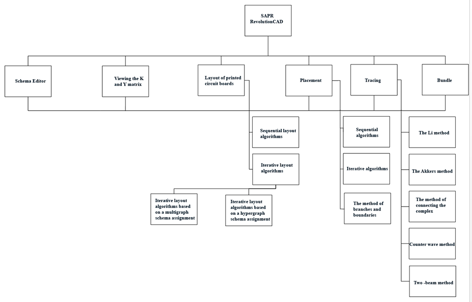
The block diagram of the CAD training is shown in Figure 1. It can be seen from the diagram that the CAD [9] training system consists of five subsystems.

Figure 1 - The structure of the training CAD scheme
Development of the branch and boundary method
The basic rules of the algorithm can be formulated as follows:
1. First of all, the subset with the number corresponding to the smallest value of the lower estimate of the objective function is subjected to branching.
2. If a condition is met for some i-th subset, then its branching [10] must be stopped.
3. The branching of a subset stops if the optimal solution found in the problem.
4. If, somewhere, the optimality conditions are met for the best acceptable solution found by this moment. The rationale is the same as paragraph 2 of these rules.
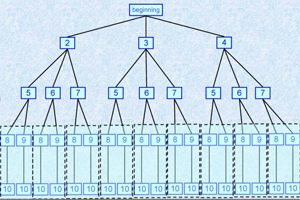
5. After finding at least one acceptable solution to the original problem, the possibility of stopping the algorithm with an estimate of the proximity of the best of the obtained acceptable solutions to the optimal one can be considered, an example of solving the solution by this method (Fig. 2).

Figure 2 - Example of solution execution by the method of branches and boundaries
The main ways of branching:
-Splitting the set of options into subsets using the "width" method and selecting the branching vertex by the minimum (maximum) of the evaluation function.
-Splitting of a set of variants according to the "in depth with return" method, i.e. sequential construction of branches.
-A combination of the two methods considered.
The method of branches and boundaries as a reduction of a full search
The basic idea of a complete search is to sort through all possible arrangements of elements on the printed circuit board in search of the optimal one.
The advantage of this method is the guaranteed finding of the optimal placement.
This method of branches and boundaries is one of the main methods of directional search, the use of which in solving the problems of placing electronic components on a printed circuit board makes it possible to find a global extremum. This method is of particular interest since, with its modification, it is possible to implement the integration of the optimality criterion.
The main idea of the method of branches and boundaries is the splitting of the entire set of acceptable solutions to the problem into some subsets, within which an ordered review of solutions is carried out in order to select the optimal one. The search process, accompanied by splitting the solution field and calculating the lower bounds, continues until all solutions except the optimal one are excluded (Fig. 3).

Figure 3 - Flowchart of the algorithm of the method of branches and boundaries
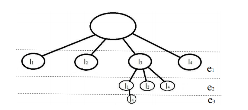
The differences in the modification of the general method in relation to the problem of placement (quadratic assignment) differ in the ways of calculating the lower bounds of the functional by the ways of splitting the field of solutions. Figure 4 shows a part of the tree of the complete decision tree.

Figure 4 - Branches and graphs of the branch and boundary method
An arbitrary placement of elements corresponds in the complete tree to some path originating from the initial vertex. For each vertex of the tree, you can calculate the lower bound of the objective function for the set of paths associated with this vertex.
If in the process of moving through the tree the lower bounds are not calculated and, accordingly, no tree truncations are made, then the method of branches and boundaries is reduced to a complete search
The following ways of cutting off branches can be distinguished:
1) Comparison of the estimate with the value of the objective function for the solution already found. The reference solution can be obtained by an approximate algorithm in advance or in the course of solving the problem using branch and boundary methods.
2) Comparison of two estimates.
Literature
1 В.В. Муленко учебное пособие для студентов вузов «Компьютерные технологии и автоматизированные системы в машиностроении». - РГУ нефти и газа им. И.М.Губкина, М., 2015. – С. 3
2 Н.П. Курочка, В.Н. Шипилов, Б.А. Шиянов научная статья «Задачи оптимального размещения ресурсов организации» - Воронежского государственного технического университета 2009
(https://cyberleninka.ru/article/n/zadachi-optimalnogo-razmescheniya-resursov-organizatsii/viewer)3 В.М. Бондарик «Система автоматизированного проектирования» уч.пособие Мн. БГУИР, 2006- 46 с.
4 В.Е. Алексеев, В.А. Таланов «Графы. Модели вычислений. Структуры данных» Учебник Нижний Новнгород,2004 – 12 с.
5 А.В. Григорьев Методы поиска новых решений в специализированной инструментальной оболочке для создания интеллектуальных САПР Десятая национальная конференция по искусственному интеллекту с международным участием КИИ-2006 (25-28 сентября 2006г., Обнинск): Труды конференции. В 3-т. Т.3. -- М.: Физматлит, 2006. С. 1031-1046.
6 И.М. Трифоненко, Н.В. Горячев, И.И. Кочегаров, Н.К. Юрков Обзор систем сквозного проектирования печатных плат радиоэлектронных средств Трифоненко И.М., Горячев Н.В., Кочегаров И.И., Юрков Н.К - Пензенский государственный университет
7 Норенков И.П. Основы автоматизированного проектирования: Учеб.для вузов / И.П. Норенков. - М.: Изд-во МГТУ им. Н.Э.Баумана, 2002.-336 c.
8 СабунинА.Е.Altium Designer. Новые решения в проектировании электронных устройств / А.Е. Сабунин. — М.: Солон-Пресс, 2009. – 432 с.
9 Горячев Н.В., Проектирование топологии односторонних печатных плат, содержащих проволочные или интегральные перемычки / Н.В. Горячев, Н.К. Юрков // Труды международного симпозиума "Надежность и качество". 2011. Т. 2. С. 122-124.
10 Горячев Н. В. Опыт применения систем сквозного проектирования при подготовке выпускной квалификационной работы / Н. В. Горячев, Н. К. Юрков // Известия ПГПУ им. В.Г. Белинского. Физикоматематические и технические науки. 2011. № 26. С. 534–540.

