Abstract
Development and researches of system of the automated designing
of composite microprogram devices of management.
The author's abstract of work of the master.
The head: senior lecturer Kovalev S.A.
The author: Danilov M.V.
INTRODUCTION
The given work sets as to itself the purpose the automated development
of devices of microprogram management, namely KMUU, with their
further realization in basis FPGA. Automated it is necessary
to understand as words, that process of development
will be somehow facilitated. In the given work for achievement
of an object in view use of pseudo-language by means of which
coding the microprogram of the automatic device would be carried
out is supposed. As Wednesday of debugging and carry on FPGA
use known CAD environments - VHDL is supposed. In other words
the received software product will represent the compiler language
of the description of microprograms - VHDL a code.
The reader can have questions of type: and what for in general
the given software product if by means of VHDL it is possible
to execute the same (actually similar questions any programmer
before the beginning of the new project) is necessary should
set to itself. To give reason for necessity of the given program
I shall bring some reasons.
Though VHLD also has appeared enough for a long time not all
him} know. And proceeding from simple mathematical calculations
it is possible to draw a following conclusion: to learn{teach}
language containing some syntactic designs (language of the description
of microprograms is very simple) much easier, than that which
contains them some hundreds (normal language of a high level).
By the way, if someone for religious or other reasons is not
pleasant VHDL to receive simply a code and for other software
products.
As it has already been told VHDL is universal language and consequently
by development on it there are complexities connected with transfer
of designs of language in hardware decisions. The result of work
of the given software product will represent a code containing
only logic operands and consequently can be interpreted only
by the unique image.
One more advantage follows from the above-stated also - the received
code can be easily optimized, and the main thing it is possible
to be assured, that it will be in appropriate way coded in FPGA.
Well and at last there can be the last (in my opinion) the remark
- digital automatic devices do not represent any interest from
the moment of occurrence of microcontrollers. I shall dare to
disagree with this statement. From the moment of occurrence of
microcircuits of programmed logic - COTTON VELVET and FPGA, many
hardware decisions are issued and debugged with their use. And
though the volume of a crystal in modern SBIS reaches millions
of gates, the volume occupied by the decision on a crystal on
former plays very important role. And I am assured, that nobody
will argue with that statement, that in connection with an occupied
place and speed no microcontroller can compete to the microprogram
automatic device (there is an opportunity to sew up the microcontroller
in crystal FPGA).
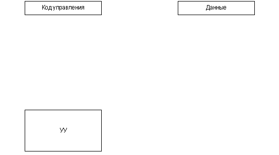
Figure 1. The block diagram of the operational
device (animated). BASES OF MICROPROGRAM MANAGEMENT
The principle of microprogram management is offered in 1951г.
M. Vilksom also assumes presence in any digital system of the
device of management (DM), coordinating work of all blocks
of system. The executive part of system which is carrying out
data processing, refers to as the operational automatic device
(AD), and the digital system as a whole refers to as the operational
device. The algorithm of work of system is set by one of formal
methods, in practice of engineering designing language of columns-schemes{-plans}
of algorithms ГСА is most widely applied.
The algorithm of management of system is set by the code of
management acting in УУ from an environment. The algorithm of
management ОА refers to as the microprogram, whence there was
a name of a principle of M. Vilks.
The microprogram can be presented in the form of sequence of
the microcommands stored in special operating memory and representing
certain image organized bit line. Such approach generates automatic
devices with "programmed" logic or microprogram devices
of management (MDM).
For formation of the sequence of sets of microoperations Y (0)
distributed{allocated} in time, Y (1)..., Y (t) where t - time,
is necessary to have the information on background of work of
the scheme. This background is represented with sets of logic
conditions X (0), X (1)..., X (t - 1), acted on input MPA during
the previous moments of time. Thus,
Y (t) =f (X (0), X (1)..., X (t - 1), X (t))
The above-stated functions are bulky and practically they cannot
be realized is hardware, especially at presence of cycles with
unknown number of recurrences. For storage of background of work
of the scheme the conditions of system forming set of conditions
A = {a1 are used..., aM}. Conditions are coded by codes K (am)
word length R?] log2M [, using internal variables Tr T = {T1...,
TR}. Codes K (am) are stored{kept} in register RG, and during
the moment of time t=0 in RG the code of an initial condition
a1 is stored{kept}. Code K (a1) enters the name in RG on signal
Start and usually is zero. For change of a code of a condition
in RG the functions of excitation forming set are used? = {?
1...? R}. For the task of the moment of change of codes of conditions
(switching) the automatic device signals of synchronization Clock
are used.
Recently, with development of microcircuits of programmed logic
- COTTON VELVETS, use and designing of final automatic devices
with "rigid" logic, has received the second breath.
Though characteristics of microcircuits constantly improve,
the problem of optimization of scheme CA remains traditionally
actual. The successful decision of this problem{task} allows
to receive cheaper digital schemes{plans} that are especially
important at mass production of the equipment.
ENCORE OF MATRIX LOGIC
The purpose of the given section is acquaintance with technologies
of programmed logic schemes existing on today.
SPLD (Simple Programmable Logic Devices), Simple programmed logic
devices. On architecture these COTTON VELVET share on subclasses
of programmed logic matrixes PLM (PLA - Programmable Logic Arrays)
and programmed matrix logic PML (PAL - Programmable Arrays Logic,
or GAL - Generic Array Logic).
Both these of a subclass of microcircuits realize disjunctive
normal forms (DNF) switching functions, and their mainframes
are two matrixes: a matrix of elements and a matrix of elements
OR, included consistently. Structural model PLM and PML are those.
Technically they can be executed and as sequence of two matrixes
of elements OR - NOT, but variants with sequence of matrixes
And - OR and with sequence of matrixes EITHER - NOT - OR - are
not functionally equivalent, To. The second variant according
to a rule where too realizes Morgan DNF, but for inverse values
of variables.
Let's notice, that the term "matrix" designates in
this case no more than "set", "set" and is
caused by that circuit elements PLM and PML is the most convenient
to have in the lines and columns, providing with that a regularity
of structure the ENCORE.
PLM - PROGRAMMED LOGIC MATRIXES
Structure PLM
Base structure PLM can be seen in figure 4, where m, l, n -
parameters PLM
On inputs of the first matrix act т entrance variables in the
form of both direct, and inverse values so the matrix has 2т
entrance lines. On its outputs conjunctive terms, which rank
not above т are formed. In the further for brevity conjunctive
terms refer to simply as terms. The number of terms has no direct
communication with size т is design data of a matrix - number
which we shall designate through l. The first matrix is identical
for both approaches SPLD. For PLM and PML.
Terms act on an input of a matrix OR. These matrixes for PLM
and PML are various. In PLM the matrix OR is programmed, and
in PML it fixed.
FPGA - THE LOGIC MATRIX PROGRAMMED BY THE USER
In the given section, we shall in details consider architecture
FPGA, to the most important class (for today) from all family
programmed SBIS.
FPGA (Field Programming Gate Array) - the logic matrix programmed
by the user is similar CPLD, turned out inside out.
As shown in Figure 5, the logic is broken into a plenty of programmed
logic blocks which individually are smaller, than PLD. They are
allocated along all chips on set of programmed interrelations,
and all file is surrounded by programmed blocks of input/conclusion.
Programmed logic block FPGA has fewer opportunities than typical
PLD, but chip FPGA contains much more than logic blocks, than
CPLD the same size.
The logic block with a reconstructed configuration
The most important programmed elements CLB - generators of logic
functions - F, G, both H. And F and G can execute any combinational
logic function from four inputs, and H can execute any combinational
logic function from three inputs.
As well as in CPLD, trapezoid fields in Figure 6 represent programmed
multiplexers. Pay attention, that conclusions F and G just as
additional inputs CLB can be directed to inputs H by multiplexers
M1 - M3 so probably to realize some functions more than four
from inputs{entrances}. The taxonomy of functions which can be
realized F, G, and H in only thing CLB, is given below:
Any function up to four variables, plus any other function up
to four untied variables, plus any third function up to three
untied variables.
Any one function of five variables.
Any function of four variables, plus another functions of six
untied variables.
Functions up to nine variables, including check of parity for
two 4 bit inputs.
At corresponding programming multiplexers M7 - M8 and M12 -
M13, conclusions of functional generators can be directed on
conclusions X and Y CLB, or they can be fixed{recorded} on D
- triggers FF1 and FF2. The trigger can use front or a cut of
the general that gets out multiplexers M9 and M14. They can use
also a signal of the sanction of synchronization, EC, chosen
M10 and M15. Sources EC and three other internal signals get
out of a set of four inputs{entrances} C1 - C4 multiplexers M3
- M6 from above CLB.
Outputs XQ and YQ CLB remove outputs of triggers from CLB. If
trigger are not used in CLB, multiplexer M11 or M16 can choose
XQ or YQ to be " a conclusion of detour " which is
simply a copy of input CLB chosen M4 or M6.
The marked block " S/R control " from each trigger
determines, the trigger in a configuration is established or
dumped{installed or dumped;established or reset;installed or
reset}. It also defines, whether the trigger answers a global
signal of installation/dump (is not shown) or on signal SR CLB
chosen by multiplexer M5.
The block of input-output
Structure of the block of input-output (IOB). Contact of input-output
can be used for input or output or both.
Contacts of input/conclusion contain started by front D - the
trigger chosen by multiplexers M5 - M7.
The programmed block of connections
As we have shown in Figure 5, everyone CLB in FPGA is introduced
in the structure connected to a network which really is only
wires with programmed connections. Figure 8 gives a little
more detailed scheme{plan} of connections. Wires really "do
not belong" to any CLB.
The number in each arrow specifies number of conductors ways
of a signal. Thus, we can see, that CLB has two conductors (conclusion)
which go to CLB below and to the right of data. It also incorporates
to three groups of wires above, one below, and to four at the
left. Signals on these wires can flow in any direction.
Four signals in group " Global Clock ", are optimized
for use as inputs of synchronization to CLB, providing a short
delay. Two groups " Singles " are optimized for maintenance
of flexible connection between adjacent blocks.
Probably to connect CLB to another, being further than one "flight",
using "Single" wires, but they should pass the programmed
switch for each flight that adds a delay. Wires in groups " Doubles " pass{take
place} two CLB before coming on the switch so they provide shorter
delays for longer connections.
For really long connections, groups " Long " do not
pass any programmed switches in general; instead of this, they
pass completely through the chip and cope elements with three
conditions nearby CLB.
Similarly to CPLD, FPGA the prices are made by flexibility of
architecture and stability of the results received from assembly
after small changes in design. There is nothing sadder than to
bring little change in big to design and to find out, that it
any more does not correspond to requirements of synchronization.
Thus, manufacturers FPGA have learned to provide "additional" resources
in architecture to guarantee stable results.
|