Burnell West and Tom Napier
Schlumberger Technologies -ATE Division
1601 Technology Dr.
San Jose, CA 95110-1397
ABSTRACT
This paper describes a novel digital functional test system architecture in which the timing and waveform generation hardware work with a sequence of events in the same manner as an IC timing/logic simulator.
INTRODUCTION
As the complexity and pin count of VLSI integrated circuits have exploded, test program generation has become immensely more complicated. VLSI semiconductor manufacturers are using the data from the simulation of these complex IC's to generate timing information and test vectors for the test program. In most cases either the input data to, or output data from the simulator must be modified, before timing and test vectors can be generated with this simulation data. This is primarily due to the difference in the technique in which the simulator and test systems handle wave-form generation.
Timing/logic simulators work with transitions in the input and output waveforms to the IC which are called events (i.e. event driven simulation). Test systems generate waveforms by trying to fit a certain format around these transitions and then programming the time at which these transitions are to occur with edges from a timing generator. The IC simulation is not restricted to using formats or limiting the number of transitions that occur in a period of time. Often a simulation will contain waveforms that the test system can not produce. One solution is to perform a special simulation in which the input data to the simulator has been modified so that the simulation will not contain waveforms that cannot be produced on the test system. Another approach is to modify the simulation output to make the data fit the test system. Modifying the input or output of the simulation has several negative effects:
- Increases test program generation time.
- Reduces the accuracy of the test by diverging from the intent of the simulation.
- Increases debug time if modifications to the simulation output create errors.
This paper introduces a new and novel ATE architecture, Sequencer Per Pin, in which waveforms are
generated in the same manner as a timing/logic simulator. We will describe how the Sequencer Per Pin architecture allows waveforms to be generated from the simulation data using an event sequence concept. Because this is the same concept as used by the simulator no modifications are necessary to make the simulation fit the test system architecture. This architecture reduces the test program generation time, while insuring that the intent of the simulation is performed during testing. The Sequencer Per Pin architecture also makes generating hand coded test programs more straight forward and faster.
BACKGROUND
When digital functional automatic test equipment first became popular in the latter part of the 60's, its architecture was very straightforward. Latches written by controllers formed the stimulus for the device under test, and comparators on the outputs would verify the device response. The standard paradigm for digital functional test was embedded in the ATLAS language statement "DO_DIGITAL_TEST", with the logical image of test functionality represented by the diagram of Figure 1.
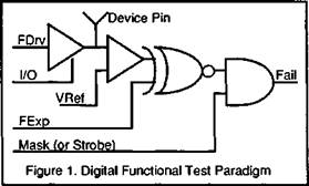
The device is driven by FDrv if enabled by I/O. Otherwise the device output is compared to FExp as long as the signal Mask (or Strobe) permits. Each succeeding digital functional test consists of the following sequence of events:
- Establish the device inputs.
- Wait for the device to respond.
- Check the device outputs.
For each device pin, at any given instant in time at most one of the following state changes can occur:
- Drive to HIGH
- Drive to LOW
- Drive OFF
- Begin Test for HIGH
- Begin Test for LOW
- Begin Test for Z-State
- End Test
Complexity arises because different pins require different sequences of events, and the timing at which the state changes are to occur will in general vary from pin to pin.
Test system architectures in the sixties and seventies evolved to minimize the hardware required to effectively produce large sequences of pin events. This was necessary, because good test hardware is costly. The principal architectural innovation of that period was the separation of functional data from timing, resulting in the development of very deep pattern memory applied with shared timing generators (TG's).[1] The functional data appeared as tables of 1's and O's (test vectors). Very effective functional tests could be produced for complex devices with just a few timing generators connected to pattern data by multiplexers and formatters. But this architectural construction, effective as it was at that time, introduced difficulties of its own. As devices became more complex, the process of parsing the test requirement into the pattern table and the timing became increasingly difficult. Limited numbers of timing resources inevitably imposed increasingly stringent restrictions on their use. The translation from the simulator output to the test program became increasingly more obscure and problematical. At the same time, device speeds dramatically increased, which made test margins ever more difficult to obtain. Pin skew and timing generator distribution skew began to dominate tester performance considerations.[2]
During the last decade, TG-per-pin test systems were introduced to help alleviate some of these problems.[3-6] As more and more resources are applied independently to each of the device pins, fewer and fewer machine restrictions are imposed on the functional test program. But simply applying a TG per pin does not eliminate the translation problem. The need to modify the simulation data exists regardless of whether the test system has shared resource timing or TG-per-pin timing architecture. The TG-per-pin architecture allows the flexibility to generate independent waveforms on
every device pin, but still restricts the waveforms with tester oriented formats and limited transitions. Furthermore, many of the available TG-per-pin systems do not provide calibrated edge placement on all functions. Thus manual changes to the timing are still required to get adequate yields. These restrictions are removed by providing each pin with a full test event sequence capability.
SEQUENCER PER PIN
We define an 'event' to be a pair (s,t), where 's' is a state and T is the time associated with a transition to 's'. An 'event sequence' is a time-ordered list of such pairs. For example, the waveform in Figure 2 here:
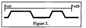
is defined by the event sequence (D1,1),(D0,8),(D1,13),(D0,18), interpreted as:
- Drive to HIGH at T=1
- Drive to LOW at T=8
- Drive to HIGH at T=13
- Drive to LOW at T= 18
The seven event types identified earlier are sufficient to define any digital test completely. Clearly, such a list can be derived directly from a simulator output. The goal is to apply this simulator data directly to the device. This goal is achieved simply by applying appropriate event sequences, as defined by the simulator output, to each pin independently. For this, we need a full sequencer for each pin. A Sequencer Per Pin circuit contains the local memory, local memory addressing, event timing generation, drive and strobe edge generation, event sequence memory, hardware calibration circuitry, strobe comparison, and fail storage logic. Each Sequencer Per Pin circuit is independent of all other pins.
For convenience in pattern storage and human comprehension of the test sequence, we do not dispense with the concept of F-data entirely. Also to reduce the amount of storage allocated to time values, the concept of global test period is reintroduced. However, the global test period is no longer a statement of how fast the device is running; it becomes nothing more than a convenient method of subdividing the test. This results in the architecture shown in Figure 3.
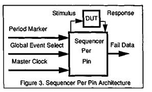
The Sequencer Per Pin circuit receives a global period marker and global event selection. The global event takes on the appearance of a 'test vector' as defined by the test systems of earlier architectures. We will use these terms interchangeably, but the reader is cautioned to keep in mind the distinction. These signals, together with the master clock, keep all pins synchronized. The stimulus waveforms generated by each Sequencer Per Pin are sent to the pin electronics in the test head. Each Sequencer Per Pin also receives the DUT output data for comparison after it has been compared to preset thresholds by the pin electronics in the test head. The period marker consists of a period time zero event which is synchronized with the master clock, together with a period vernier value which tells the Sequencer Per Pin precisely when within the clock period the event sequence is to begin. The resolution of the period vernier is the test period resolution (not, as in many earlier architectures, the master clock it-self). Clearly, with this arrangement, there is no need to manipulate the master clock frequency to achieve desired stimulus pattern rates, with the consequent test program complications.
IMPLEMENTATION
The Sequencer Per Pin circuit is implemented in a total of eight custom integrated circuits. The heart of the circuit is an ASIC which performs the event generation and timing. Six calibratable linear delay elements using ECL technology for speed and stability are used to achieve the required high resolution and accuracy. A local memory control IC is implemented in CMOS. A pin slice PCB contains four Sequencer Per Pin chan-nels.[7-8]
Since the local memory, timing, waveform generation, and calibration circuits are all contained on a single board the configuration of the system is very modular and easily configured to the user's needs. Also, this partitioning minimizes the number of system interconnections and therefore improves the overall reliability.
The high speed sections of the system are liquid cooled to insure their reliability and stability. A cold plate is attached to each card and a specially designed heat sink transfers the heat from each component on a board to the cold plate. The cold plate is cooled by refrigerated FC77 liquid circulating through copper tubing. This ensures that the junction temperature on any IC will never exceed 85° C. A low stable junction temperature will greatly decrease component failure and improve accuracy by preventing component timing from drifting due to temperature changes.[9]
CONCLUSION
A revolutionary tester architecture, the Sequencer Per Pin architecture, has been described. This architecture implements tests as sequences of events for each pin, synchronized by global period markers. This allows for performing complex tests on VLSI integrated circuits without requiring extensive program development and debug efforts. The automatic generation of these complex waveforms and strobe placement from timing simulators was not possible on the prior generations of ATE. In addition, this architecture is more flexible than previous designs, permitting more precise implementations of simulation data with fewer restrictions. The Sequencer Per Pin architecture will decrease the time needed to generate test programs by reducing the manual intervention required to generate timing and test vectors from timing/logic simulation data. The event sequence concept allows significant reduction in test pattern storage requirements, and optimizes this feature even further by permitting run-time assignment of pin data, avoiding duplications of test patterns and test programs for different package configurations.
Reference:
- Herlein, R.,'Optimizing the Timing Architecture of a Digital LSI Test System', \TC Proceedings, pp. 200-205, 1983.
- Sugamori, S., Yoshida, K., Maruyama, H., Kamata, S. 'Anaylsis and Definition of Overall Timing Accuracy in VLSI Test System', ITC Proceedings, pp. 143-153,1981.
- Bisset, S., The Development of a Tester-Per-Pin VLSI Test System Architecture', ITC Proceedings, pp. 151-155, 1983.
- Sudo, T, Yoshii, A., Tamama, T, Narumi, N., Sak-agawa, Y. '"ULTIMATE": A 500-MHz VLSI Test System with High Timing Accuracy', ITC Proceedings, pp. 206-213, 1987.
- Chang, Y, Hoffman, D., Gruodis, A., Dickol, J., 'A 250 MHZ Advanced Test System' ITC Proceedings, pp. 68-75, 1987.
- Grasso, L.J., Morgan, C, Peloquin, M., Rajan, F., 'A 250 MHz Test System's Timing and Automatic Calibration', ITC Proceedings, pp. 76-84,1987.
- Tamama, T, Narumi, N., Otsuji, T., Suzuki, M., Sudo, T, 'Key Technologies for 500-MHz VLSI Test System "ULTIMATE"', ITC Proceedings, pp. 108-113, 1988.
- Muething, R., Saikley, C, 'Integrated Pin Electronics: A Path Toward Affordable Testing of High-Pin Count ASIC Devices', ITC Proceedings, pp. 883-887, 1987.
- Sakagawa, Y, Akazawa, Y, Narume, N., Yoshii, A., Sudo, T, 'Packaging Technologies for 500-MHz VLSI Test System "ULTIMATE"', ITC Proceedings, pp. 120-124, 1988.
[источник]
|
 Cвистунов Сергей Николаевич

