Автор: Aaron Schultz
Ссылка на источник:http://www.commsdesign.com/showArticle.jhtml;jsessionid=UVS0QPAPMJKU4QSNDLOSKH0CJUNN2JVN?articleID=16503626
Random Jitter - What Is Really Going On?
Introduction
Anyone involved in fiber optic communications continuously hears people talk about random jitter. Random jitter is one of those terms like broadband that has meaning to people who are skilled in the technology, but may be just a buzzword to newcomers. What is random jitter? Of course there are countless books and papers on the subject. It is beneficial to highlight the often overlooked key mathematical underpinnings of random jitter as it relates to communications links, and to evaluate the most widely used measurement methodologies.
A wide range of professionals need to consider random jitter. Designers at the system, module, and chip levels need to be concerned with what degradations signals with undergo from point A to point B. Random jitter is one example of degradation that erodes bit error rates at all component and system interfaces.
Random jitter is specified in the way it describes clock edge fluctuations. Accordingly, jitter is typically listed as an amount of one clock period, or an amount of one unit interval (UI). Should the edge of a clock jitter around over time 10 picosecond (ps) within a 100 ps clock period, then the jitter is 0.1 UI.
Any jitter that describes how much in time a clock edge varies can be given as a peak-to-peak number. Peak to peak jitter specifications are convenient when the jitter is deterministically characterizable. But as random jitter is probabilistic, it is difficult to say what the maximum jitter can possibly be.
In fact, for Gaussian random jitter probability density functions (PDFs), there theoretically is no limit to how much deviation there might be between the proper and actual time of a clock edge. Fortunately, the PDF suggests that large deviations in clock edge times are highly improbable.
Random jitter is typically described by RMS rather than peak-to-peak UI since there theoretically is no maximum. A 0.01 UI RMS random jitter measurement informs that the standard of deviation statistic of clock edge deviations is 1 % around the ideal clock edge time.
Measurement
The following three methods prevail when measuring random jitter:
Time domain: Instruments such as oscilloscopes perform histograms on the times when clock edges pass through mid-range voltage values.
Data eye opening: A bit error rate tester (BERT) samples a bit stream at different times within a clock period. The probability of error changes as the data are sampled at different times with respect to their rising and falling edges.
Frequency domain: Instruments such as spectrum analyzers reveal imperfections in clocks by looking at how the frequency content deviates from a single spike at the center frequency.
Let's focus on these three random jitter measurement methods from mathematical and practical standpoints, with the goal being to create a concise, informative picture how to describe and measure random jitter.
Time domain random jitter
How does random jitter affect the performance of a communications link? In other words, how does the variability in zero crossing affect a receiver's ability to resolve "1s" from "0s"? Consider the decision making system of Figure 1. At the time of a clock rising edge zero-crossing, the receiver decides whether the data waveform is a "1" or "0." So long as the noise around the signal is small enough that the signal still is above or below a threshold, then the receiver's guess will be correct.

Should the noise be large enough compared to the signal strength, then a false reading may occur. The strength of signal compared to the amount of noise present is called the signal to noise ratio (SNR). The probability of error depends on the SNR: the higher the SNR, the less the probability of error.
One convenient metric used in calculating probabilities of error with Gaussian noise PDFs is the error function, sometimes called erf(x). The error function evaluated at x will say how much probability there is for an outcome of a random variable with 0 mean and 1 s to lie between 0 and x, or between infinity and x (depending on which version of erf(x) is used). In a system where the signal is either S or -S, and the Gaussian noise standard of deviation is s, the probability of error can be shown to be:

with erf(x) as used in MATLAB software. As the SNR S/s increases, the error function increases, and the probability of error decreases. The following table gives some Pr(error) results for different SNRs.
| SNR (raw) | SNR (dB) | Pr(error) |
| 4 | 12.0 | 3.2 * 10-5 |
| 5 | 14.0 | 2.9 * 10-7 |
| 6 | 15.6 | 9.9 * 10-10 |
| 7 | 16.9 | 1.3 * 10-12 |
| 8 | 18.1 | 6.1 * 10-16 |
Figure 2 helps to illustrate the relationship among time jitter, SNR, and probability of error. Sampling the data waveform at its zero-crossing yields a 0.5 probability of error (worst case) because there is zero signal. Assume the data waveform is a line with slope m V/s in the vicinity of the data zero-crossing. Then the signal S is mt at time t away from the zero-crossing. The probability of error at time t is less in equation (1) because the signal S is larger.
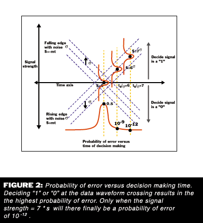
In order to achieve a probability of error of around 10-12 as desired in many present day communications systems, there needs to be a SNR of 7. The data waveform must be sampled at a time after tS/s=7 for a bit error rate < 10-12. Exactly when after the data waveform zero-crossing SNR=7 depends on the rise time due to the slope m.
Due to the assumption of linearity of the waveform, the time at which the voltage is 7 * s is 7 * sj, with sj being the RMS jitter. Hence one can say that a voltage SNR of 7 is needed for Pr(error) = 10-12, or alternatively that the decision point must occur at least 7 * sj after the data zero-crossing for this probability of error.
Herein is where the probability of error and the time jitter are linked. That the decision point must occur beyond +/- 7 * sj around the data zero-crossing means that there is (14 * sj) / T(sup>0 UI of random jitter with respect to a bit error rate of 10-12 (T(sup>0 being the nominal bit period). Statements like this one capture the true essence of the purpose of jitter.
Histograms such as in Figure 2 can be generated on sampling oscilloscopes. RMS random jitter is thus directly measured in the time domain. Sometimes peak-to-peak jitter is discussed in addition to RMS. Many texts relate peak-to-peak jitter to 14 * sj. Peak to peak jitter is the maximum time deviation of a zero-crossing. Since jitter is probabilistic, theoretically there is no limit to the max time of a crossing. The 14 * sj is not so much a true peak to peak jitter as much as a measure of how much of a decision making window will yield Pr(error) > 10-12.

Eye opening
Measuring RMS jitter using time histograms as previously shown is easily done in the lab. And in theory, knowing the time domain RMS jitter gives a good idea of how much time within a bit period will yield Pr(error) > 10-12.
However, as jitter is specified not for its own sake but ultimately for predicting link performance, a different way to measure jitter would be to create a link and measure empirically actual bit error rates by making the decision across a bit period.
This method yields results that do not depend on theory. Measuring a bit error rate by sweeping a decision making clock across an entire bit period produces plots such as Figure 3. The shape of the plot is sometimes referred to as a bathtub.
On the bathtub curve, one can identify all the time during which decision making is expected to yield a Pr(error) > 10-12. This time is called random jitter, by definition. Random jitter, though modeled by Gaussians as in the previous section, is in its purest and most informative essence the time during which, due to randomly distributed noise sources, the probability of error is higher than some threshold. The rest of the bit period, in which Pr(error) < 10-12, is called the eye opening.
Assuming that the empirically measured random jitter can be modeled by a Gaussian, then RMS jitter can be inferred from random jitter measured using this method by dividing by 14. The advantage of this method over the time histogram method is the directness of the result. Random jitter measured by virtue of the bathtub is precisely the time over which the Pr(error) is too high. Time domain measurements can only predict this time by multiplying an RMS by 14.
This method of jitter measurement may give more pessimistic results than the time domain. The good news is extra jitter in clock sources derived from the application chipset for clocking in data will be veritably observed. The bad news is extra jitter at error detector inputs may give rise to additional eye closure beyond jitter specifically in the clock and data signals. A thorough engineer needs to know the jitter inherent in the test system.
Frequency domain
Not surprisingly, as jitter is typically specified with respect to a time period, it is also possible to discuss jitter in the frequency domain, specifically phase with respect to 2s radians or phase noise. One can equate RMS time jitter in UI -- the standard of deviation of time deviation with respect to one clock period -- to RMS phase angle jitter -- the standard of deviation of phase deviation with respect to one 2s phase cycle.
In particular, for any time deviation, there is a corresponding phase deviation given by:

with Dt being the time deviation, T(sup>0 being the nominal bit period, and Df being the phase deviation from 2p radians. Using probabilistic math methods (2), the following equation relates the phase noise to RMS time jitter:

To find the time RMS jitter sj, then, one could conceivably measure the phase noise variance sf2 and then use equation (3). Then, the question is how to measure the phase noise variance?
One question might be: How is the phase noise specified? Phase noise -- how far the phase of a signal at a given time varies from what it is supposed to be -- can affect a signal at any frequency. For example, consider a 622 MHz square wave. There might be phase noise at 10 kHz.
This means that the phase of the 622 MHz waveform will be modulated at 10 kHz. This phase modulation (can be translated to frequency modulation) produces sidebands in a frequency spectrum of the waveform. Comparing the energy in these sidebands at 622 MHz +/- 10 kHz to the energy at the 622 MHz frequency indicates how affected the carrier is by phase noise.
Hence it is typical to specify phase noise as energy with respect to the carrier at an offset frequency from the carrier, for example --130 dBc at 10 kHz away from 622 MHz.
A spectrum analyzer shows how much energy is contained in a signal versus frequency. One can read off the phase noise by comparing relative strength of energy at frequencies offset from the carrier to energy at the carrier. The units of the energy spectrum is dB / Hz.
Normalizing to the carrier energy, then the spectrum is dBc / Hz. An integration of the energy under the curve except for the energy at the carrier yields the sum total of all phase noise energy with respect to the carrier energy (dBc without the Hz). This integrated energy total can be shown to be generally related to the variance of the phase noise sf2 by

with S(s) being the spectrum measured on the spectrum analyzer EXCEPT for the energy at the carrier (dBc/Hz). Then, using equation (3), the RMS time jitter can be found using this measured phase noise variance. Since only energy in the sideband is being incorporated in the phase noise, the limits of integration change per Equation (5).

with f0 being the smallest frequency deviation away from the carrier (for example 10 kHz, so f0 = 622.010 MHz), and f1 being the largest (for example 10 MHz, so f1 = 632 MHz).
Thus the relationship between phase noise and RMS time jitter is shown. An advantage of the phase noise measurement method is its lack of dependence on any particular noise model. There is no Gaussian assumption for the source of the phase noise. Phase noise variance is a black box metric. And there is no need to relate using rise and fall times voltage noise to phase noise.
However, it may be difficult to read accurately on a spectrum analyzer the dBc of the spectrum and then to integrate. And even when this measurement is doable, there is the question of how close in frequency to the carrier to stop integrating. Any energy that is not precisely at the carrier frequency represents phase noise.
In practice low frequency jitter in signals (energy very close to the carrier frequency in an energy spectrum) is usually irrelevant because phase lock loops (PLLs) can successfully deal with lower frequency input jitter. As a result, it is not uncommon to specify and integrate phase noise from, for example, 10 kHz and higher away from a carrier.
Random jitter, method comparison
The following table lists the advantages and disadvantages of measuring random jitter using the three methods.
| Method | How to measure | Advantages | Disadvantages |
| Time domain | Histogram on sampling oscilloscope |
Easy to measure with scope
Directly read off the RMS jitter |
Assumes Gaussian noise model.
Questionable accuracy since scope inputs have some amount of jitter already. Questionable relevance to a peak-to-peak random jitter related to a bit error rate, especially when the data edges start to round off before SNR is high enough. May not account for time-created jitter. Gives no versus frequency information that might separate random from non-random jitter. |
| Eye opening | Bit error tester with sweepable decision making time |
Directly gives the random jitter with respect to a bit error rate, which is the real purpose of a jitter specification. Completely independent of noise models. |
Need to set up a bit error rate tester, and sweep the sampling point through an eye. This takes time and requires expensive equipment.
Jitter at the error detector input may obscure accuracy Gives no versus frequency information that might separate random from non-random jitter. |
| Phase noise | Integrate the area under an energy versus frequency plot from a spectrum analyzer, then convert to RMS time jitter. |
Independent of noise models. Will reveal all phase noise. Can convert to RMS time jitter. |
Questionable relevance to a peak-to-peak random jitter related to a bit error rate.
Question of how near to the carrier to stop integrating phase noise. |
Hopefully we have clarified random jitter as it relates to communications links. Three methods of understanding random jitter are presented - time domain, eye opening, and frequency domain. Unfortunately, no one method is entirely perfect or complete. The good news is once one can understand random jitter from these different perspectives, and once one can understand how the different methodologies are interrelated, one can more effectively make sound, appropriate engineering judgments while implementing communications systems.
Aaron Schultz is a principal applications engineer at Quake Technologies Inc. He can be reached at aschultz@quaketech.com.
References
- Stephen B. Alexander, Optical Communication Receiver Design, The International Society for Optical Engineering and The Institution of Electrical Engineers, 1997.
- Athanasios Papoulis, Probability, Random Variables, and Stochastic Processes, Third Edition, McGraw-Hill, Inc., 1991.
- Todd Charles Weigandt, Low-Phase-Noise, Low-Timing-Jitter Design Techniques for Delay Cell Based VCOs and Frequency Synthesizers, Engineering-Electrical Engineering and Computer Sciences Ph. D. thesis for the University of California, Berkeley, Graduate Division, 1998.
- R. E. Ziemer and W. H. Tranter, Principles of Communications -- Systems, Modulation, and Noise, Houghton Mifflin Company, 1990.