Тематическая статья №4
FPGA Co-Processing Solutions for High-Performance Signal Processing Applications
Авторы:
Tapan A. Mehta, Strategic Marketing Manager, Altera Corporation
Joel Rotem, Chief Application Engineer, MangoDSP
Описание: На протяжении последних лет высокопроизводительные приложения для обработки сигналов, такие как получение изображений в медицине, передача видео на расстоянии, военные приложения и приложения безопасности начали адаптироваться к гибридной архитектуре, которая состоит из ПЛИС и DSP (процессор для обработки цифровых сигналов). В статье рассмотрены методы реализации DSP на основе ПЛИС.
Источник:
http://www.altera.com/literature/cp/gspx/fpga-coprocessing.pdf
FPGA Co-Processing Solutions for High-Performance Signal Processing Applications
Tapan A. Mehta
Strategic Marketing Manager
Altera Corporation
101 Innovation Dr., MS: 1102
San Jose, CA 95148, U.S.A
(408) 544 – 8246
Email: tmehta@altera.com
Joel Rotem
Chief Application Engineer
MangoDSP
2107 N. First Street, Suite 310
San Jose, CA 95131, U.S.A
(408) 437- 2234
Email: joel@mangodsp.com
Overview
Over the course of the past few years, several high-performance signal-processing applications, such as medical imaging, video broadcast, security, and military have started to adopt a hybrid architecture, which consists of FPGAs and digital signal processors. Historically, these high-density digital signal processing (DSP) applications have been delivered through “DSP farms” where many digital signal processors were arrayed together to deliver parallel DSP. The advent of DSP-capable FPGAs, however, has resulted in a surge of signal-processing performance that has redefined the architectures of high-density DSP systems.
FPGA Co-Processing Solutions
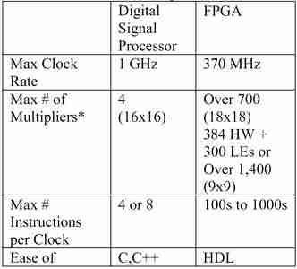
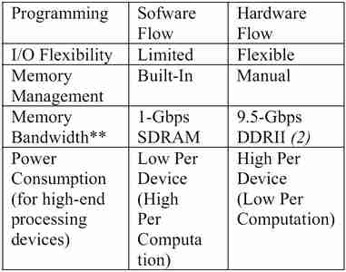
A common architecture for signal processing combines the inherent advantages of digital signal processors and FPGAs to yield ultra-high performance and highly flexible signal-processing systems. The advantages of digital signal processors include high-clock rates (currently up to 1 GHz), C/C++ language-based development, built-in memory management, and built-in I/O interfaces. The disadvantages include a limited number of instructions/clocks, a limited number of multipliers, fixed word sizes, and fixed I/O interfaces. Most digital signal processors allow very limited inter-processor communication, relying on low-speed buses, such as peripheral component interconnect (PCI), to connect to other digital signal processors. The advantages of FPGAs include a high number of instructions per clock, one to two orders of magnitude more multipliers, and flexible word size. For example, the new Altera ® Stratix® II FPGA family has up to 384 18X18 multiplier/ accumulators per device, each running at 370 MHz, as well as nearly 180 K standard logic elements (LEs). FPGAs allow memory access to fast memory devices, such as double-data rate (DDR), DDRII, RLDRAM and quad data rate (QDR). Furthermore, FPGAs can be connected together, and to other devices such as digital signal processors, via Gbps high-speed LVDS and multi-gigabit serializer/deserializer (SERDES) buses. The disadvantages of FPGAs include longer development time, increased device power (but not on a computational basis), and clock rates about one-third the peak of DSP processors.
Table 1. DSP/FPGA Comparison


Notes:
* Multipliers can be implemented using hardware (HW) based multipliers and logic element (LE)-based multipliers.
**(2) Other memory interfaces are supported, including single-data rate (SDR), DDR, DDRII, RLDRAMII, QDR, and QDRII.
After reviewing Table 1, it can be seen that the two devices compliment each other. While digital signal processors are ideal for rapid development of new and complex algorithms, they are limited to running two or four calculations at a time. FPGAs can perform mathematical operations on an entire vector or matrix at the same time. Furthermore, FPGAs are ideal for connecting multiple processing nodes together, distributing the data between digital signal processors and collecting and recombining the sub-calculations into a single output stream.
An architecture composed of FPGAs and DSPs can be optimally utilized in the many applications listed in the overview. The medical diagnostic imaging application is a very good example of an FPGA and digital- signal-processor-based architecture. This paper will discuss the medical application developed by Mango DSP using Altera’s Stratix FPGAs combined with TI’s C64xx processors.
Case Study: Computed Tomography (CT)
Computed tomography (CT) imaging (also known as computed axial tomography (CAT) scanning) provides an example application of where and how these high- performance DSP and FPGA systems are being used. CT is one of the fastest-growing modalities and has proven to yield much better results than the decades-old x-ray procedure. CT imaging can be used across several emerging applications, such as cardiovascular, virtual colonography, and neurology. CT has gained this position based on its ability to deliver high- resolution images in a short amount of time.
In CT imaging, the patient lies on a gurney and is rolled into a giant “donut” ring. While the patient holds extremely still, the large ring rotates around the patient, emitting low- dose radiation from one side of the ring while a linear array of sensors detects the absorption of the ray-trace on the opposite side of the ring. During each revolution, the CT machine takes a 3D cross-sectional view called a slice. Each slice consists of a thousand or more images, which are taken at sequential radial intervals. After each revolution, the ring moves a small distance down the body and another revolution of images is taken. In this way, a huge amount of data is collected that can be reconstructed into a high-resolution, 3D image of the hard and soft tissue inside the body.
Two cornerstone technologies for CT are the power slip ring and high-performance image processing. The power slip ring enables continuous revolutions of the scanner around the patient’s body without slowing down. This technology replaced a system where the scanner could only make a single revolution and then had to reverse directions so that the attached power and data cables would not tangle around the axle. The power slip ring enabled a huge increase in the rotation speed of the ring around the patient, significantly lowering the time it takes to capture a high-resolution image, while also greatly increasing the processing bandwidth required to absorb and process the generated data. The second revolution has been in image-processing technology, enabled by high-speed DSP and FPGA signal processing devices.
The typical CT system includes a signal processing dataflow from data acquisition, filtering, back projection, image reconstruction, and display. Figure 1 shows the typical CT imaging flow.

Figure 1. CT Imaging Data Flow
The first stage of the digital unit of the CT is data acquisition. The unit is hooked up to hundreds of sensors providing digitized readings of radiation levels. The acquisitions require a high-speed programmable interface with a data buffer capable of collecting the samples and streaming them to the system. Data acquisition from analog sensors nearly always requires some type of filtering operation. In CT, the filtering is performed in the frequency domain, thus requiring a fast Fourier transform (FFT) followed by a finite impulse response (FIR) filter. This image transformation and filtering are performed by the FPGAs.
Back projection provides the heart of the algorithmic processing in CT and other similar imaging applications. Back projection transforms the x-ray vector and attenuation information, the sinogram, collected through all scans to reconstruct the 2D image and 3D image. The basic algorithm used in back projection is the inverse radon transform. This transform takes the sinogram and transforms it into a 2D reconstruction of the soft tissue densities in the body cross section.
The inverse radon transform requires considerable processing performance. The processing requirements are composed of three major variables, the number of views, the number of pixels, and the number of images per second. Typical numbers today are 1000 views multiplied by 1,000,000 pixels multiplied by 15 images per second, which equals 15 billion operations per second. In the future this will reach 4000 views multiplied by 4,000,000 pixels multiplied by 30 images per second, or 48 billion operations per second. Figure 2 shows a simplified version of back projection.

Figure 2. Computed Tomography (CT) Back Projection
The inverse radon transform must be performed pixel by pixel and does not lend itself well to vectorization. For each pixel in the image, the processor must retrieve sample information from all the scans performed on the object and overlay them. The memory access is, therefore, not only large but also non-sequential, which can create a bottleneck in data retrieval.
The inverse radon transform is implemented with a mix of digital signal processors and FPGAs. The FPGA receives the entire data stream and segments it between the digital signal processors, providing each processor with a certain amount of pixels to compute. The FPGA must analyze and direct the correct views to each digital signal processor. The digital signal processor performs the system-state machine management, computes linear pixel-to-pixel increments in the projection plan, and controls the memory-and-accumulate module.
The processed pixels are then sent to the FPGA for final accumulation, image reconstruction, and output to monitor, typically using DVI output to an LCD screen.
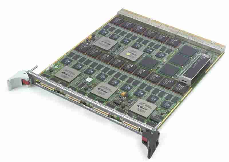
The Harrier cPCI board from Mango DSP is an example of a system that supports this digital signal processor plus FPGA co- processing architecture. The board is a cPCI board with 15 TI C6415 DSPs at 600MHz (up to 1GHz max.) and five Altera Stratix EP1S30 FPGAs with 2-GBytes SDRAM memory. The FPGAs are connected to four external I/O ports running at up to 680 Mbps. These ports can handle the data acquisition, as well as “daisy-chain” boards to build systems with up to hundreds of FPGAs and digital signal processors running simultaneously on the same data source. The board architecture is based on processing clusters, each containing one FPGA and multiple digital signal processors. The clusters are connected via a high-speed ring bus. The samples entering the board are divided amongst the FPGAs. Each FPGA performs the FFT and filtering and then divides the pixel processing between the digital signal processors. The processed information returns to the FPGAs. One FPGA then collects the processed pixels from all the FPGAs and performs the reconstruction and output. Figure 3 outlines the Harrier board architecture, and Figure 4 shows a picture of the Harrier cPCI board.

Figure 4. MangoDSP Harrier cPCI DSP Board, featuring Altera Stratix FPGAs
Summary
In the future, more and more applications will require the processing power provided by DSP-plus-FPGA co-processing solutions. The CT medical imaging application discussed in this article will continue to drive processing requirements by increasing resolutions and the need for live video viewing of the CT images to assist during medical procedures. The processing challenges in medical imaging equipment— ultra-high signal processing performance, very high memory bandwidth, and the resulting need to communicate between and coordinate many processing elements—are very similar to the market requirements in optical inspection, video broadcast, scientific computing, security, and military applications. The complementary capabilities of digital signal processors and FPGAs integrated into high-density systems will continue to evolve to meet these growing challenges of high-complexity signal processing applications.