Тематическая статья №6
Extending the Peripheral Set of DSP Processors using FPGAs
Автор: Joe Hanson, Altera Corporation, Director, System Level Tools
Описание: В статье описывается применение ПО Altera SOPC Builder для расширения периферийного набора DSP процессоров, используя FPGA, что позволяет избежать высокой стоимости нового продукта и соответствовать потребностям рынка.
Источник:
http://www.altera.com/literature/cp/gspx/peripheral-set.pdf
Extending the Peripheral Set of DSP Processors using FPGAs
Joe Hanson
Altera Corporation
Director, System Level Tools
101 Innovation Drive
San Jose, CA 95134
(408) 544-7810
jhanson@altera.com
As the cost of new product development increases, new digital signal processor (DSP) development will target either a broad range of general purpose solutions, or a specific high-volume application. When a processor is intended for a broad range of applications, it is only likely to have for 80 percent of the peripherals needed for any particular application. On the other hand, processors intended for a specific, high-volume application will have 100 percent of the needed peripherals designed in. Additional peripherals are likely to be needed to adapt either of type of product to a slightly different application, to provide the necessary level of product differentiation. FPGAs and FPGA development tools now offer ways to adapt these types of products to meet the peripherals requirements of a new application quickly and with little or no hardware description language (HDL) design.
Today’s FPGAs and CPLDs, such as Altera’s Cyclone II, Stratix II and MAX II device families, offer the performance, density and the multiple input / output (I/O) standards required to address a wide range of peripherals. The Cyclone II and Stratix II FPGA device families, for example, offer specialized DSP blocks to deliver maximum performance for DSP functions, while the low-cost MAX II CPLD family are excellent choices for I/O expansion applications. Using FPGA development tools like Altera’s SOPC Builder tool, system designers can define and integrate the peripheral subsystem without writing HDL and do it in a fraction of the time of traditional system-on-a-chip (SOC) design methods.
DSP Processor Interfaces
DSP processors today come with one of two types of interfaces: simple or complex. The complex ones include standard interfaces such as PCI, PCI-X, PCI-Express, as well as vendor-specific, high-speed solutions such as Analog Devices’ Linkport or Texas Instruments’ VLYNQ. For simple peripheral expansion, these cores add a level of complexity that may not be warranted. Simple interfaces, which include the external memory interfaces composed of address, data and control signals, on the other hand, are ideal for simple peripheral expansion and add very little in terms of system complexity. Furthermore, these simpler interfaces are available on the vast majority of standard products. The biggest challenges when interfacing to additional peripherals is dealing with the various interface standards, different data path widths, and varying number of bus cycles per transfer required by the new peripherals. Altera’s SOPC Builder tool addresses these issues.
SOPC Builder
Altera’s SOPC Builder tool, included in the Quartus II development tool, provides a table-based entry system for listing the processors and peripheral (Figure 1) components that define the system. Each of the SOPC Builder components listed in the library of components provides a file that describes the component in some form and another file that describes the interface signals and requirements for data transfers. Based on this information, SOPC Builder generates a switch fabric that contains all of the decode logic, arbitration logic, interrupt control, wait-state control and data-path matching logic that connects the processors to the peripherals. The SOPC Builder library components can be very simple blocks of fixed logic, or they can be complex, parameterized, and dynamically generated subsystems. For custom peripherals, the tool provides an import wizard to bring in the design files and map them into an SOPC Builder component.
The Avalon Switch Fabric
Instead of trying to force the whole category of peripherals to fit the same bus standard, SOPC Builder creates a switch fabric, based on the Avalon specification and optimized for peripherals used in a particular system. The Avalon specification, available for free from Altera’s web-site www.altera.com, was designed to accommodate peripheral development for the system–on–a–programmable chip (SOPC) environment. The specification provides peripheral designers with a basis for describing the address-based read/write ports found in Avalon master (e.g. microprocessors) and Avalon slave (e.g. memory, UART, and timer) peripherals. The specification describes transfers as being between the peripheral and a switch fabric interconnect. This interconnect strategy allows any Avalon master to be connected to any Avalon slave, without a priori knowledge.
The SOPC Builder tool implements this switch fabric interconnect strategy. In doing so, the burden of generating the appropriate logic to connect the various devices is moved from the engineer to the tool. As a result, this approach allows designers to focus their efforts into optimizing the peripherals and their application—the real value of the system—and minimizes their time on resolving integration issues.
External Memory Interfaces and Avalon Interfaces
With the wide variety of external memory interfaces on processors, the flexibility of the Avalon interface makes it ideal for connecting standard processors to peripherals in or through the FPGA. The Avalon interface supports asserted high- or asserted low- logic levels for any control signal. It also supports masters with up to 128-bits of address and data paths of up to 128- bits wide. Internal to the FPGA, the read and write data paths are separate non-tri-state high performance data paths.
For most processor interfaces, the external memory interface can be presented as simple wires to the FPGA and the Avalon switch fabric by just matching the processor signal types to the Avalon equivalent. The only logic required on the interface is the control logic converting the processor’s bi- directional data bus into the separate read and write data paths used by Avalon, which can be a little as a single logic element. FPGA I/O elements easily support toggle rates of 133 MHz, more than ample for the great majority processor external memory interfaces.
For the FPGA logic, the Avalon switch fabric generated by SOPC Builder provides optimal decode logic with minimum levels of logic. The performance of FPGA logic is dependent on the FPGA family, the types of peripherals and the number of peripherals connected to the Avalon switch fabric. With today’s FPGA high performance peripherals sub-systems are readily achieved.
External Memory Interface (EMIF)
The external memory interface (EMIF) on TI DSP devices map directly to Avalon signal types (Figure 2) The EMIF allows the FPGA-connected peripherals to function in the same way SRAM access allows the peripherals to insert wait-cycles through the use of the ARDY signal. The generation of the ARDY signal is automatically handled by SOPC Builder and the Avalon switch fabric. The ADDRESS[25:0] signals map to the Avalon address[] signal type. The other control signals, AWE_n and ARE_n map directly to the Avalon write_n and read_n signal types. The nOE is used with the CS (chip-select) signal to further qualify a read from a write transaction and to control the direction data (DATA[31:0]) mapping on to the Avalon write data and read data paths. If addressing individual byte support is needed, the BE[3:0] signals map to the Avalon byte-enable signals. Figure 3 shows the simple Verilog description of the interface, excluding the port and signal declarations.
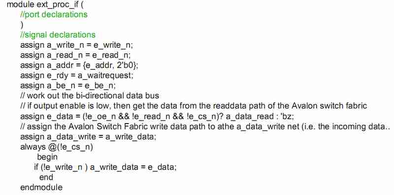
Figure 3 Verilog for EMIF to Avalon Interface
User Defined Peripherals
A hardware engineering team can design unique custom peripherals independent of the processor selected. SOPC Builder fully supports user-defined components through its interface–to–user logic wizard (Figure 4). The wizard imports the user’s design file (or files) to read the port list. The user simply maps the module’s signal names to equivalent Avalon signal types. Once the mapping is complete, the designer selects the timing page to define the number of clocks or any setup and hold-times required for read and write transactions. With this information, SOPC Builder can create an appropriate switch fabric that allows any master peripheral to exchange data with this custom peripheral. By publishing the component to the library of components, the component is made available for easy re-use in the same system or other new systems without making any changes to the peripheral.
Simplifying Multi-Master Processor Design
The SOPC Builder approach also makes it simple to add a soft-core processor, such as the Nios II processor, to off-load the host processor or add DMA controllers to move data around within the FPGA. SOPC Builder provides the designer with a table that shows all the processors and peripherals in the system, as well as which processors have access to which peripherals. Peripheral sharing is simply controlled with the push of a button. Each time an adjustment is desired, the designer simply revisits the table, makes the changes, pushes the button and a new solution is generated.
Embedded Application Software
After integrating the components, the software development begins. Many of the SOPC Builder components include software drivers and sample application code for exercising the peripherals. SOPC Builder copies this software into directories for usage. SOPC Builder also generates a standard C header file for each processor in the system with the memory map and register declarations provided. Each time SOPC Builder generates a system, these files are updated. This automatic hand-off to the software team of the latest parameters and declarations with each new hardware image accelerates the system development by maintaining hardware/software coherency.
Conclusion
The escalating high cost of new product development requires new approaches to adapting standard products to meet exact product needs. SOPC Builder’s unique productivity-enhancing approach leverages the density, features, and performance of today’s FPGAs and CPLDs, to expand the peripherals set for standard processors. By implementing a novel switch-fabric interconnect, this approach provides opportunities to increase the system’s performance and add other capabilities into the system.