Тематическая статья №7
DEBUGGING AND HARDWARE VERIFICATION FOR FPGA-BASED SYSTEM DESIGN
Авторы: Mario Vera-Lizcano, John M. Espinosa-Duran, Jaime Velasco-Medina
Описание: В статье описываются возможности ПО SignalTap от Altera для отладки и аппаратной верификации систем на базе ПЛИСов. Проекты отлаживаются на целевом оборудовании с помощью встроенного логического анализатора SignalTap.
Источник:
DEBUGGING AND HARDWARE VERIFICATION FOR FPGA-BASED SYSTEM DESIGN
Mario Vera-Lizcano, John M. Espinosa-Duran, Jaime Velasco-Medina
Grupo de Bio-nanoelectronica, EIEE. Universidad del Valle. A. A. 25360, Cali, Colombia
E-mail: {mario, michaele, jvelasco} @univalle.edu.co
ABSTRACT
This article describes the use of an approach for debugging and hardware verification of FPGA-based system designs using Altera’s SignalTap. The designs are debugged and verified by executing directly on the target hardware the SignalTap Embedded Logic Analyzer (ELA), which provides high observability, controllability, and interactivity of the designs. In this case, direct hardware execution is a lot of times faster than software simulation approach, therefore the validation time is speed-up. Additionally, it allows design modifications. In this work, the 32-bits NIOS processor was used as test vehicle, which is synthesized over an APEX20KE device. As an application example, a matrix multiplication algorithm was executed and the experimental results show that Altera’s SignalTap is very suitable for in-system hardware verification.
1. INTRODUCTION
FPGA-based design is a popular way to implement hardware due to their flexibility and fast time to market. Additionally, this design approach allows to carry out a complete functional verification using configuration readback, partial reconfiguration and built-in logic analyzers. Then a fast debugging and in-system verification is achieved. FPGA vendors provide tools to achieve a high observability and controllability, which allow quickly finding and removing bugs of the designs.
As it is well know, in the classical FPGA-based system design process, the time of debugging, validation and hardware verification is critical. In this case, near to 50% of the design time is inverted in these steps, because the software simulation (commonly used for debugging and validation) is extremely slow and can take hours or days, and the implementation of a specialized debug technique delay the time design.
Today, the FPGA vendors guarantee that the devices are free of defects of fabrication, then the hardware verification is oriented to functional and time verification. Therefore, there are tools that allow in-system hardware verification, which provide the same level of observability and controllability as a software simulator, these enable designers to locate and remove quickly the bugs from the design. Observability is the ability to access all internal state of the circuit, similar to the ability of a software debugger to view the values of variables. Controllability is the ability to modify the run-time state of the circuit, similar to changing the values of program variables in a software debugger [4].
This work describes the use of SignalTap ELA from Altera, which provides complete observability and controllability for functional verification of FPGA-based system designs.
This article is organized as follows. Initially, section 2 presents an overview of debugging techniques for FPGA- based system design. In section 3, a brief description of SignalTap tool is presented. In section 4, the basic process for debugging and hardware verification is described. In section 5, the experimental results on the NIOS processor are presented. Finally, section 6 presents the conclusions and the future work.
2. OVERVIEW OF DEBUGGING TECHNIQUES FOR FPGA-BASED SYSTEM DESIGN
A similar ASIC design and verification methodology is generally used for FPGA-based system design, however several additional process or steps can be used with FPGAs, which influence and increase their advantages for system design. One of these additional process is design for debugging. In [1] are presented some debugging techniques, which include:
• Hardware execution of designs for functional and timing verification: Since there is little cost (time, mostly) in creating the FPGA programming bits for a design, a design can be implemented and executed in hardware for functional and timing verification. Simulation is still important to rid the system of obvious design flaws, but hardware execution can increase designer productivity by placing the design in a realistic testing environment and reducing execution time to seconds or minutes rather than hours or days.
• Simple design modifications to make internal signals visible: Since a design can be rather quickly modified (especially compared to ASIC design), routing internal signals to “debugging port” pins for temporary visibility can be an effective way to gain an understanding of what a design is doing under test or real conditions. These debugging signals can be 2 removed from the design before production once the design has been verified.
• Embedding extra debugging hardware into a design: Again, since an FPGA can be reprogrammed numerous times, debugging hardware can be temporarily added to designs --sometimes at relatively little cost-- to provide extra observability, controllability, or execution control for design verification, some examples of possible circuitry which might be added are:
– scan chains (for observability and controllability)
– hardware breakpointing mechanisms
– embedded logic analyzers (ELA)
– statistics gathering hardware
– self-test hardware.
The addition or modification of debugging hardware to a design is similar to the instrumentation or modification of software performed for debugging and program monitoring. Of course, performing these modifications has its drawbacks in terms of verification, the chief being that it alters the timing characteristics of the circuit and generally increases the area of the design. For instance, modifying the circuit may alter the critical paths of the original circuit, making timing verification of the original design less precise if the verification is performed using the modified circuit. To be the most accurate, of course, timing verification should be performed on an unmodified circuit.
Regarding the area costs, since the modifications are only temporary, the costs may be tolerable, except for the cases where the design will not fit in the desired FPGA size. In these cases, less costly debugging strategies may be available, such as using the FPGA’s native state sampling capabilities or routing limited signals to unallocated external pins (in space and/or time).
In trying to improve the productivity of designers, the process of modifying circuits for debugging should not only be automated but the time required to perform the modifications should be reduced as much as possible. If a designer can automatically modify a FPGA design in seconds or minutes rather than tens of minutes or hours, he should be more willing to use one or more different instrumentation techniques to characterize the circuit’s execution, thus, increasing the chances of identifying design problems quickly [1].
3. SIGNALTAP EMBEDDED LOGIC ANALYZER
The SignalTap ELA, is an Altera`s tool, non-invasive and easy to use, that helps to reduce the time of debug and hardware verification of the FPGA-based system design.
SignalTap is used as a design for debugging tool, where the designer does not need to worry about the observability and controllability of the design, because SignalTap made that work, and with the help of other tools like RTL Viewer, Floorplan Editor and Node Finder Utility, its capabilities are increased. This tool also allows to made on-line hardware verification, because is possible to observe in real-time that the designed system is doing.
3.1 General Description
The SignalTap ELA captures signals from any internal node or I/O pin of some specific Altera`s family devices: Stratix II, Stratix, Stratix GX, Cyclone II, Cyclone, APEX II, APEX 20KE, APEX 20KC, APEX 20K, Excalibur and Mercury[3], in real-time at system speed. SignalTap analysis also eliminates the need for external probes and design file changes to capture signals from an internal node. The logic analyzer control’s and signal capture display are all accessible from the Quartus II design software [5].
3.2 Functional Description
The SignalTap is a parameterized ELA that provides access to signals inside some Altera family devices. SignalTap could be parameterized to capture from 1 to 128 signals from internal nodes or I/O pins. Signal capture occurs in-system and at system speed. From Quartus II, the user selects which signals will be captured, when signal capture starts, and how many samples of data are captured. The user can also select if captured data will be stored in the embedded system block (ESB) RAM of the devices, or if data will be sent to I/O pins for capture by external analysis equipment. Data stored in ESB RAM is transferred to a host computer by using the MasterBlaster or ByteBlasterMV communication cable and is displayed in the SignalTap waveform viewer [2].
4. USING SIGNALTAP FOR DEBUG AND HARDWARE VERIFICATION
In order to improve the performance of the designs, Altera proposes a design process shown in the Figure 1. However, this approach cannot be adequate for fast-time design, then a short way of this process is use hardware verification to achieve the same goals, which is shown in Figure 2. The process is:
1. To realize time analysis using RTL Viewer.
2. To realize time improvement using Floorplan Editor.
3. To use SignalTap for hardware verification and debugging.
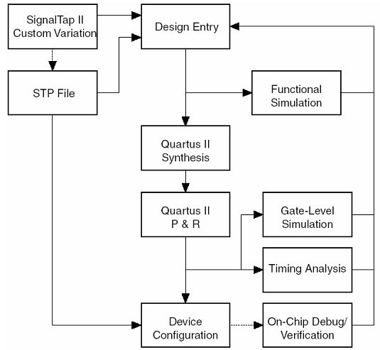
Figure 1. Altera FPGA-based system design process.
4.1 Time improvement using RTL Viewer
In order to solve the time critical path of the design this approach uses the RTL Viewer. Then, to improve the critical path is necessary to know about how the compiler of Quartus II implement the designs, in this case is recommended run the RTL Viewer, which allows to see at Transfer Register Level (functional blocks) the design and can be observed all the hierarchical level of the design until arrive to the gate or Logic Elements (LE) level. This initial step help to debug the most common time problems without using simulation, because it allows full observability of the design at any level.
4.2 Time improvement using Floorplan Editor
After run the RTL Viewer, the Floorplan Editor is used toobserve the physical implementation of the system designed over the FPGA. Then is possible to improve the timing requirements by considering re-assign I/O pins or LogicLock a block-region or moving blocks.
4.3 Working with SignalTap
To accelerate the verification process is necessary to determinate all signals, nodes and I/O pins of interest.
To add signals to the SignalTap is possible to use the Node Finder or the Floorplan Editor Utilities. The normal way to do it is using the Node Finder, which allows to select the signals generated during the compilation process, I/O pins, internal nodes and buses or signals. The Floorplan allows to access signals which can not be observed using the Node Finder, then, it allows to achieve full observability (this signals include the Boundary-Scan Registers, ESB, and all the nodes that physically exist).
When add or remove signals of the SignalTap is necessary to recompile the design. Also, there are other modifications that need recompilation such as: change the SignalTap Clock, change signal assignment, change the Sample Buffer Depth, enable Trigger Input and Output and enable the Debug Port. In the case that a signal is removed of the design it is necessary to remove it of the SignalTap file.
Finally the design is compiled and programmed on the device, then the SignalTap ELA is ready to work.
5. EXAMPLES
In this section of the work the hardware verification results are presented.
A matrixes multiplication algorithm was executed over the NIOS processor in order to verify how suitable is SignalTap for debugging and functional verification.
The algorithm was executed for N=30 (30x30 two matrixes multiplication). The NIOS custom example configuration, which allows to realize the multiplication using a customize hardware was used. The multiplier has two operands registers, a and b, each one of 16 bits, and a result register of 32 bits. The experimental results show some multiplication realized; the Figure 3 show some simulation results obtained with ModelSim in order to verify the correct operation of the multiplier; The Figure 4 show the results obtained with SignalTap in order to verify in-system the correct working of the multiplier.
Like could be appreciate, the multiplier work correctly.
A standard computer with an AthlonXp 2600+ with 512DDR-RAM using WindowsXP operating system was used to realize the probes. The simulation realized was about 100us and take near of 1 minute running. The same results doing hardware verification with SignalTap were obtained at 100us. Another advantage to use SignalTap is that if you want to verify the correct execution of an algorithm over the NIOS, just load it in to memory and watch the results in the PC. While using ModelSim you have to regenerate the model of the device for each algorithm, incrementing the design time.
The full compilation takes 4:45 minutes, while the full compilation with the analysis of 64 signals with SignalTap takes 5:40 minutes, approximately 1 minute more, but in the case that you want to implement a classical debugging/test strategy obviously you will take more time. The compilation result show that the NIOS occupied a 43%( 3658 LEs) of hardware and a 24% (26496 bytes) of memory, but the NIOS with SignalTap occupied 56% (4710 LEs) and a 55% (59264 bytes) of memory, obviously there is a increment in the hardware used, but keep in mint that this increment will be only to verify the system designed in the FPGA, then it will be removed. In the case that you do not have available memory (but have hardware available) in the device remember that the internal nodes could be wired to the I/O pins automatically through the debug port, to be connected to external logic analyzers.
As show the Figure 5, with the RTL viewer you can know how your design is implemented, so if you have a time-delay problem caused by a bad based-time design you can appreciate it and correct.
The Figure 6 shows the partial view of the NIOS from the Floorplan editor. As it is viewed the design is really sparse, so it could be putted together or relocated some parts of the design. In this work it is not made because we work with a IPcore that has many lock regions and the pins could no be reassigned because they have been assigned to work with the Excalibur Development Board from Altera.
6. CONCLUSIONS
This article presents a short approach for debugging and hardware verification of FPGA-based system design using Altera’s SignalTap.
In this work, the 32-bits NIOS processor was used as test vehicle, which is synthesized over an APEX20KE device. As an application example, a matrix multiplication algorithm was executed over a 32-bits NIOS processor which was synthesized in a APEX20KE device and the experimental results show that Altera’s SignalTap is very suitable for in-system hardware verification.
In this case, direct hardware execution is a lot of times faster than software simulation approach, therefore the validation time is speed-up.
SignalTap tool based in Boundary Scan test technique, work as a design for debugging strategy, that allow achieve observability and controllability of the system designed without that the designer know about test techniques.
The classical design process for a FPGA-based system change, because now it is not need to carry out the classical waveforms simulations to debug and verify the design, instead of that, these steps are directly executed in 6 hardware, which is faster that simulation because the designer is working with real signals at speed-system. The future work will be oriented to implement this approach in complex system designs.
7. ACKNOWLEDGE
This work was sponsored by Altera Corporation through the University Program. The authors give a special thanks to Mrs Ralene Marcoccia of Altera Corporation.
8. REFERENCES
[1]P.S. Graham, “Logical Hardware Debuggers for FPGA-based Systems”. Department of Electrical and Computer Engineering. Brigham Young University. December 2001
[2]“SignalTap Embedded Logic Analyzer Megafunction”. Data Sheet. Altera Corporation. April 2001.Ver. 2.0
[3]“qii53009-2.0 Design Debugging Using the SignalTap II Embedded Logic Analyzer”. Altera Corporation. June 2004.Ver. 2.0
[4] T. Wheeler, P. S. Graham, B. Nelson, B. Hutchings “Using Design-Level Scan to Improve Design Observability and Controllability for Functional Verification of FPGAs” Department of Electrical and Computer Engineering. Brigham Young University.
[5] H. Latorre-Ossa. “Test en Linea de Sistemas Implementados en HCPLDs”. Undergraduate Thesis. Escuela de Ingenieria Electrica y Electronica. Universidad del Valle. 2003