Тематическая статья №8
When Probing Goes in the Chip
Автор: Joel Woodward, Agilent Technologies
Описание: Особенности зондирования современных ПЛИС, достоинства и недостатки такого подхода.
Источник: http://www.soccentral.com/results.asp?EntryID=13186
When Probing Goes in the Chip
Contributor: Agilent Technologies, Inc.
May 2, 2005 -- Today's system-on-chip designs create a situation where system complexity, coupled with time-to-market pressure, make the debug and characterization of these systems more critical and challenging than ever. At the same time the physical implementation in making the traditional measurements needed has become nearly impossible. The answer is instrumenting SOC designs with on-chip probing technology.
BGA packaging brought with it a new era where probing individual components directly became impossible. Probing innovation moved from an emphasis on connecting with individual packages to PC board connectivity. And while today's physical probing solutions can accurately measure busses running in excess of 1 GHz on PC boards, the technology has not addressed the need for the probes to extend inside the chip.
Why the need? With the adoption of digital systems-on-chip in full swing, entire sub-systems that used to be implemented on circuit boards are realized inside a single device. Since the individual devices and busses that interconnect them are now "buried" inside the chip, it is no longer possible to probe and acquire data for integration of hardware subsystems, hardware and software integration, and performance characterization.
While exhaustive simulation has been the primary verification tactic for SOC designers, simulation alone is not sufficient. The slow nature of simulation constrains teams to testing just a small fraction of real-time operation. With sub-nano second edge speed running around the chip and on the board, there are a number of issues nearly impossible to simulate because the models don't have the subtle detail that would be necessary. And when design teams move from simulation to a physical prototype, they lose needed internal visibility.
Route-out Approach
Teams using FPGA technology are luckier than their ASIC counterparts due to the reprogrammable nature of FPGAs. Many FPGA designers employ a "route-out" approach for design visibility. Early in the design the team dedicates a limited number of pins for debug. To probe a subset of internal signals, the team routes out these signals to pins. Each time the team wants to probe new signals, they must change the HDL design to bring out new signals, re-synthesize the design, and then run place and route. Additionally, each time the design changes to probe new signals, the team must configure and set up an external logic analyzer or scope so that it is wired correctly to the debug port and has the correct signal names entered in the instrument. Even through changing internal probe points may take several hours per iteration and has the negative consequence of affecting design timing, it is quick compared to the cost and time required for ASIC technology and remains a key method of getting internal visibility.
Both the difficulty and number of iterations a team makes can be reduced by implementing on-chip probing. On-chip probing complements PC board probing by extending virtual probe tips into the chip. Criteria that should be considered when designing or selecting commercial on-chip probing should include:
- The ability to implement on-chip probing as an afterthought as well as early in the design process
- The ability to keep timing constant as new probe points are selected
- The number and type of incremental device resources used
- The amount of time and expertise required to change probe points
On-chip Resource Consumption
For on-chip measurement with an external logic analyzer or scope, the most expensive on-chip resource will be IO. The number of IO available for debug will always be substantially smaller than the number of internal signals a design team would like to measure simultaneously. To best exploit the limited number of pins available for debug, on-chip probing begins with the addition of a switch or multiplexer (MUX). Crossbar switches require many routing resources making multiplexers a better choice.
Multiplexers, a key component to on-chip probing, allow the team to trade off routing and logic resource consumption for better visibility. Let's look at the example of a team that has dedicated 8 pins for debug. The team could implement eight 2:1 MUXes to simultaneously view 8 signals out of 16 choices. While keeping the design constant, the team now has access to 16 signals over just 8 pins. The team could commit more routing and logical resources to make eight 4:1 MUXes giving them access to 32 signals over the 8 debug pins. Or the team could use a 2X DDR implementation to implement sixteen 4:1 MUXes to provide access to 64 signals over the 8 debug pins. With a few tradeoffs in available on-chip resources, visibility ports can become more effective.
On-Chip Probing and Device Timing
Minimizing the changing of device timing is critical for on-chip probing. This can be a source of frustration to designers as adding an internal probe point can cause the timing of the design to change. Suppose a designer wants to route out a signal in the bottom-left hand quadrant of his chip, and the debug IO are located in the upper right hand corner of the chip. The place and route tools know that the latency associated with the path from the signal being probed to the IO must be less than one clock cycle. If the device speed is fast enough, the place and route tools will want to "pull" the logic block that contains the signal closer to the debug pin IO so that it can meet timing. This then causes changes to other parts of the design. A good way to minimize timing effects is for on-chip probing to implement pipelining. The addition of on-chip probing will have minimal impact on design timing due to its pipelined architecture. Multiple flops can be placed between the signal being probed and an output pad (see Figure 1). The design tools place the first flop as close as possible to the signal being probed. The additional stages of pipelining allow the signal multiple clock cycles before reaching the output pad. Multiple signals being probed simultaneously would each have the same number of pipeline stages. The pipelined architecture of the on-chip probe allows the place and route tools to have a much greater probability of meeting the original timing goals of the design. As this approach is synchronous, the place and route tools eliminate skew between signal paths rendering a valid bus measurement.
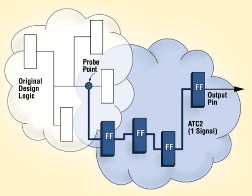
Figure 1: Xilinx and Agilent collaborated to develop an on-chip probe for FPGAs. A pipelined architecture uses four stages to route a signal to the debug port. This automated approach gives place and route tool flexibility to meet timing requirements. The router can use timing solely within the on-chip probe core, known as ATC2, to move across the chip
Probing Control
Being able to easily determine and change what signals are being probed is critical. One method is to set register values that determine which inputs of a MUX are probed. This approach requires greater emphasis of on-chip probe implementation during design and a higher level of design understanding during debug.
An easier method is to use existing JTAG port to control each MUX to select which signals are probed. For FPGA technology, this requires an understanding on the JTAG scan chain and JTAG controller implemented by the FPGA vendor. Access to this information is easier to get for commercial on-chip probing solutions and more difficult for individual design teams that wanted to use JTAG for on-chip probing control.
Agilent's FPGA dynamic probe provides a good example of how JTAG can make probing selection easy for virtually any member of the design team. Agilent's on-chip probing core, ATC2, is a special MUX that can be configured with anywhere from 1 to 64 input signal banks. Each signal bank is equal in width to the number of debug pins a team has reserved. From the interface of an Agilent logic analyzer or oscilloscope, in two mouse clicks, a team member can select which input signal bank is active, thereby changing internal probe points (see Figure 2). Application software running on the instrument communicates via a JTAG cable with the on-chip probe using the instrument's USB or a parallel interface.

Figure 2: Agilent and Xilinx have teams to create the first on-chip probing solution for FPGAs. Application software running on an Agilent logic analyzer or oscilloscope sends a command via JTAG to configure internal MUX selections. This has the effect of changing which internal signals can be measured by the instrument in less than a second without requiring the user to be intimate with the design itself.
Smart On-chip Probes
On-chip probing provides some unique opportunities that have not previously been available in traditional physical probes. Additional on-chip circuitry can be developed to make the probe "smarter." For example, keeping trace of where a team is probing can be challenging. The designer must remember what signal is being probed, which physical pin it was routed to, how that pin connects to a logic analyzer or scope, and enter the signal name in the instrument using the correct channel mapping. This process is tedious and prone to errors and must be repeated each time internal probe points are changed.
2005 saw the introduction of the very first commercial solution to solve this issue. The on-chip probe core, in addition to the basic MUX structure, also contains simple stimulus ability. It produces a training pattern on its output pins, one at a time. The instrument looks for this unique pattern on any of its acquisition channels. When the instrument finds the pattern, it associates that instrument channel with the on-chip probe output pin producing the training pattern. It then repeats the process for each of the remaining output pins eliminating the need to manually enter probe layout information.
Commercial vs Team Design of On-chip Probing
For ASIC technologies there are currently no commercial on-chip probing technologies that can be deployed across a wide range of designs. The reprogrammable nature of FPGAs and the higher volumes of FPGA design starts make this a more fertile technology for commercial and proprietary implementations of on-chip probing. In addition to on-chip probing technologies, like Agilent's FPGA dynamic probe, that connects external measurement equipment to the inside of the chip, there are several available solutions where the instrument, in the form of IP, goes in the chip. On-chip probing technologies now serve as a front end to these measurement systems.
Probing Other Components Through the FPGA
As FPGAs take on more system capabilities, they are often wired to other key components on a PC board. Using on-chip probing, users have access to all post-synthesis signals in the FPGA. While it may be impossible to physically connect to a specific board component, the user can easily access component pins provided that the component is connected to the FPGA. This provides a method of accessing and measuring a greater number of components from the FPGA itself and can minimize the number of special connectors for probing.
SOC design visibility required for effective system validation has begun spawning on-chip probe technologies. Implementing on-chip probing increases the team's ability to get wide internal visibility to quickly and effectively validate system designs.
By Joel Woodward, Agilent Technologies
Woodward received his BSEE from Brigham Young University, an MBA from Regis University, and has done graduate work at Harvard University. For the past 16 years Joel has worked at Agilent Technologies (Hewlett-Packard) as an engineer and manager on development tools within the EDA and test and measurement industries.