
 |
Burkhovetsky Denis |
|
Faculty of Computer information technologies and automation Department of automation and teleautomatics Theme of attestation work of «Research of analog PLL in a digital communication channe» Scientific Leader professor Voroncov Alexander Grigorievich |
||
Abstract of the work:
«Research and optimization mode for capturing analog PLL synchronization systems TCS»
The rapid development of digital switching systems and means of transmitting information resulted in a significant increase in the role of synchronization in telecommunication networks.
In the synchronization system is often used PLL system, char-acteristics which often make the most important contribution to the synchronization system.
Objective: Improve the structure and parameters optimization of analog PLL system as a slave sync.
Tasks:
1) Assess the value and place of synchronization systems in modern telecommunication networks.
2) justify the use of an analog PLL to synchronize the system;
3) Perform a comparative analysis of methods and tools for capture in analog PLL;
4) Implement improvements to the block diagram of the network and on the model in SystemView show its efficiency and effectiveness.
5) Consider alternative solutions, to compare with those obtained before the results and conclude the feasibility of implementing these innovations.
Scientific novelty
The scientific novelty of this work is to implement an analog PLL with a nonlinear in the control circuit, as well as a comprehensive analysis of the behavior of a system such as a separate element, as well as an integral part of the network synchronization.
Expected practical results
As a result of this work is planned to obtain analytical and experimental data to develop recommendations for the creation of an analog PLL for synchronization systems of telecommunication networks, also planned to obtain a workable model in a package SystemView, which would allow for the characteristics of the systems and network synchronization and further evaluation of their quality.
1. Synchronization Systems in modern telecommunication networks.
Synchronization - a tool to maintain the operation of all digital equipment in the communications network at a high speed. For digital transmission of information is converted into discrete pulses. When sending these pulses through the line and communications digital network, all its components must be synchronized. Sync must exist on three levels: bit synchronization, the synchronization at the level of timeslots and Framing.
The main purpose of network synchronization is to limit the emergence of controlled slippage. There are two main causes of slippage. The first reason is the absence of the clock rate due to loss of connection between the generators, which leads to a difference in clock frequencies. The second reason - or phase shifts in the lines of communication (such as Jitter and Wander), or between primary and driven generators. The latter, that is phase shift between the frequencies of the primary generator and receiver, as shown above are the main cause of slippage in communication networks.
Slippage, however, are not the only failures, caused by-governmental lack of synchronization. Bad timing can lead to excessive jitter and frame loss in the transmission of digital signals.
To synchronize the digital network uses several basic methods: Plesiochronous work, hierarchical work unit - the transmitter, mutual synchronization, pulse addition (stuffing) and pointers.
To synchronize the networks E1/DS1 most administrators telecoms networks uses the method of hierarchical power - with-the transmitter (master-slave). The source of the main reference signal syn-chronization of the network is one or more primary reference generator (PRG). The reference signal generator that is distributed over a network consisting of generators - receivers or slave master oscillators (SMO).
The node with the most stable generator node is assigned a source. Node - the source transmits synchronization reference to one or more receiving nodes. The performance of the host sites are usually the same or worse than the source node. Node receiver captures the reference clock frequency source and then transmits it to other sites receiver. Therefore, synchronization is distributed down the hierarchy of nodes.
The most important demand generators in the receiver is the possibility of perestroika (restructuring) maintain synchronization. This is explained by the fact that the generators receiver can often be prone to brief interruptions of the reference clock signal. A brief interruption causes the restructuring of the generator. Restructuring is defined as switching the generator to the reference signal or to introduce a small error in the duration.
Characteristics of synchronization in a hierarchical network of the transmitter-receiver are determined by three components: the error control generator, the characteristics of devices distributing the reference signal, and the characteristics of the generator unit, receiving the reference signal through these devices. Characteristics of the synchronization is mainly determined by the combination of characteristics of distribution devices and a generator unit. In real networks, the generator unit, connected to the control generator, will work with long-term rate that differs from the frequency control generator.
In the synchronization system is often used PLL system, char-acteristics which often make the most important contribution to the synchronization system.
Loops sync issues when the generator is used to track your own reference clock signal. In the event of such loops, the frequency of the reference signal becomes unstable. Generators in the loop synchronization slowly begin to work with an error of the full range of the generator. This leads to the fact that the generator shows the characteristics many times worse than in free mode or on hold. It is therefore important that the flow of the reference clock signal in the network would be designed in such a way as to synchronize the loop could be formed under any circumstances. No combination of primary and / or secondary reference signals should not lead to a loop synchronization. In a well-planned network is always possible to avoid the loop synchronization.
Keeping the hierarchy is important for achieving the best workers ha-tics in the network. Under ideal conditions or under stress transfer sync with the best in the worst generators optimizes performance.
Characteristics of the synchronization will always be worse, because Timing is transmitted from generator to generator. The more generators and equipment in the chain synchronization, the greater the accumulated deterioration and the greater the frequency shift. Each unit will add deterioration, which will have to respond generators in the chain. Therefore, to ensure the best characteristics of chain synchronization should be short.
2. Feasibility of using an analog PLL synchronization systems
Phase-locked loop PLL is often necessary to use the systems of data transmission over the air synchronization for receiving and transmitting equipment.
PLL is used:
a) to eliminate the phase jitter (phase jitter) in digital data transmission systems appearing on the edges of the digital signal;
b) to increase the sensitivity of the receiver;
a) to highlight the clock frequency of the received signal;
d) to synchronize the receiving and transmitting equipment.
PLL adjusts the clock frequency allocated to the received signal at the right time. PLL decides correction after a certain number of discrepancies in the up or down. If the prevailing differences in the smaller side, then the PLL extends the duration of the signal formed. Otherwise, the PLL inserts an additional shorter pulse. Thus there is a synchronization and selection of clock frequency of the received signal.
Can be used as analog and digital PLL. Each of them has its advantages and disadvantages, which we will try to merge, creating a more universal system.
Phase-locked loop (PLL) is a widely used kind of node, which is produced by some firms in a separate IC. PLL contains a phase detector, amplifier tel and voltage-controlled oscillator (VCO), and a combination of analog and digital technology.
There is the traditional bias against the PLL, which is partly due to the complexity of the implementation of the PLL on discrete components, and partly based on the assumption that the PLL can not reliably work. However, the appearance is now a large number of inexpensive and easy to use device allows the PLL to quickly remove the first obstacle to their widespread use. If the device PLL properly designed and used to limit the parameters, it is as reliable circuit elements, as an operational amplifier or trigger.
Phase detector comparison frequency cornfield two input signals and generates an output signal, which is a measure of the phase mismatch (for example, if they differ in frequency, it will form a periodic output signal of difference frequency). If the frequency fvh and fgun not equal to each other, then the signal of the phase mismatch after filtering and amplification will affect the gun, bringing the rate to fgun fvh. In normal mode VCO quickly produces a «capture» the frequency fvh, maintaining a constant phase shift with respect to the input signal.
Output VCO generates a signal with a frequency fvh, while it is «clean» copy of the signal fvh, which itself may be susceptible to interference. Since the output periodic signal VCO can be any form of triangular, sine, and so n.), It gives an opportunity to form, say, a sinusoidal signal, synchronized with posledvatelnostyu input pulses.
Often used in the PLL counter modulo n, is included between the output VCO and phase detector. With this meter are frequency multiples of the input reference frequency fvx. This is useful for forming clock pulses to synchronize the system.
In this paper, an experiment was conducted, during which we compared the quality of digital and analog PLL under different noise levels. Up to a certain level of noise digital PLL works better than analog in the case of small noise yields zero error. But then, with further increase in noise, the number of errors increases dramatically and the system quickly becomes unusable. At that time, as an analog PLL continues to operate, and the number of errors on the noise level depends almost linearly (Fig. 2).
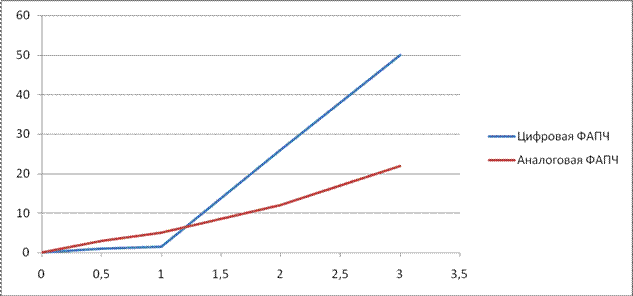
Figure 2 -Dependence of the probability of erroneous reception of noise in the digital and analog PLL
This experiment confirms the hypothesis that the analog PLL works best with strong interference.
3. Designing the structure of analog PLL nonlinearity in the control circuit.
A common characteristic of the PLL system contradiction between the expansion of the capture bandwidth and increase their filtering ability. Indeed, narrowing the band problowing the filter in the chain of control and reducing the bandwidth of retention, can significantly increase the filtering capacity of the system. However, as previously shown, inevitably reduces capture bandwidth.
One solution to this problem is the introduction of nonlinearity in the control circuit (in the Low Pass Filter) in order to increase the capture bandwidth of the system while maintaining its high noise immunity
The essence of this method increase the capture bandwidth with ¬ standing in the use of different levels of the variable component Bdriven to the output of the phase detector in the regime of beats and on hold for a weak interference. In this case, the filtering capacity of the system for weak noise can significantly increase (without reducing the capture bandwidth), if the filter is built in such a way that when a strong signal (active beat), he had a broad band and a weak signal (on hold) - narrow. This condition can be implemented in various schemes of the filter. In particular, Yu Eltermanom proposed single-stage scheme of integrating filter (Fig. 3), consisting of the usual linear capacitor and a nonlinear resistor.
Nonlinear resistor, as shown in Fig. 3, Consists of a linear resistor connected in parallel and included two meet each other diodes D1 and D2 with the sources of confining the displacement of U1 and U2. By adjusting the value of locking bias can change the length of the linear portion of the current-voltage characteristics of the nonlinear resistance.
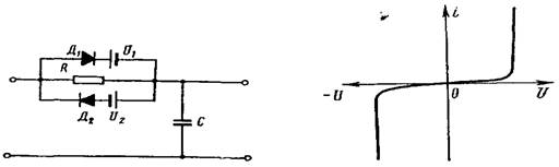
Figure 3 - The scheme of nonlinear Figure 4 - Volt-ampere charac-
RC-filter tics of the nonlinear element
Non-linear integrating filter can be performed using a linear resistance and nonlinear capacity.
We describe the system mathematically, by replacing the nonlinear part of the scheme the nonlinear resistance and adding a system of R1 and Rng. To simplify the calculations we take into account the instantaneous resistance Rnel.
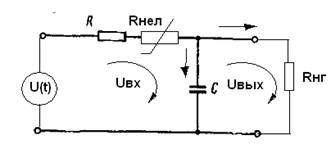
Figure 6 - Scheme nonlinear RC filter
-iвх+ic+iвых=0
R1iвх+Uнел(iвх)+Uc(ic)=Uвх
Uвых-Uc=0
The nonlinear element has the VAC
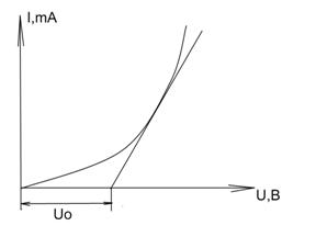
Figure 7 - VAC nonlinear element
After a tangent to the operating point, we can see that a certain section of the curve and tangent are approximately equal to the angle of inclination, and therefore the value Rnel = will be approximately equal, and when considering the curve, and when considering the tangent. Therefore, at this stage nonlinear element, we can replace the two linear elements. Moreover, this change will be equivalent.
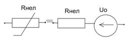
Figure 8 -Replacing the nonlinear element
Then, by the 2 nd Kirchhoff's law:
(Rнел+R1)* iвх +Uвых +U0=Uвх
Create the meta, (hereinafter called its modulus 1), which simulates the transformation of the input voltage to output.
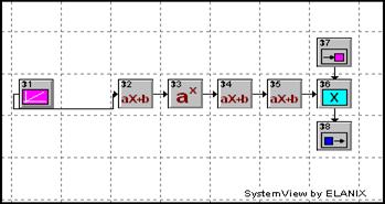
Figure 9 -Realization of the nonlinear voltage conversion in the PLL control circuit in the package SystemView
Module 1 has been integrated into the original scheme of PLL and investigated according to the probability of an erroneous signal from the noise in the original circuit PLL (P (0)) and the PLL circuit with the module 1 (P '(0)). Yielded the following relationship:
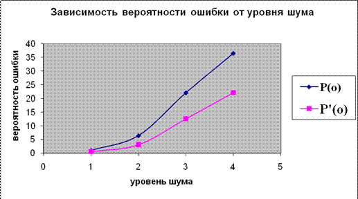
Figure 10 -Dependence of error probability on the noise level
As can be seen in the average system with innovations gives the gain in average 150-200%.
If we compare the result with the original scheme of an analog PLL, which at STD deviation of noise = 3 gave the error probability = 22%. In the new system with STD deviation of noise = 3, error probability = 12%.. And with the noise STD deviation = 4 system was workable only in theory receive an error = 36%, in a system with module 1 - the probability of incorrect acceptance is 22%. The digital system is not working with STD deviation = 3.
Was also investigated another variant of realization of the nonlinearity - using block with a dead zone. When comparing the 2 systems (with substantial non-linearity and the module 1, it was found that the capture system gives almost the same, but in terms of noise immunity is better scheme with modulus 1 (1,5 -2 times)Because the scheme with a significant nonlinearity weakens the power of the signal passing through it and rebuilt rather low
In the future:
1. Bring to the end of the study PAFC systems with substantial nonlinearity and the module 1.
2. Make all results in a master's work.
![]()
![]()