
Abstract
Contents
- Introduction
- 1. Theme urgency
- 2. Goal and tasks of the research
- 3. Development of FPGA-based SoC verification methodology
- Conclusion
- References
Introduction
Design of digital devices is inextricably linked with the concept of verification. The concept of verification in generally means a test of coincidence of the results of the developed device and the requirements that are presented to them. Verification takes more than 60% of the total design time [1] and attracts most of the employed staff. Existing methods of digital devices design verification are used only at finished product debug level. With this approach, even a small error, inscribed in an early stage, may lead to more serious consequences in the future, which usually mean additional material and time costs. With current methods of design up to 70% of errors occur during the initial stages of design and only the final stage of device debugging can eliminate about 70% of errors, which was made earlier [2]. This situation is shown on fig. 1.
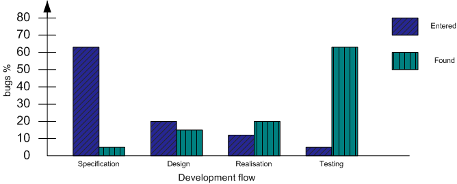
Figure 1 — Distribution of errors in current methods of designing
This situation is further exacerbated by the fact that the technological capabilities of the design and verification are significantly behind the level of complexity of modern digital devices. The dynamics of technological capabilities in relation to the possibilities of CAD and verification tools is shown on fig. 2.
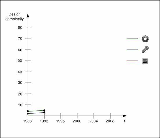
Figure 2 — Current dynamics of technological capabilities
(animation: 6 frames, 5 cycles of repetition, 140 KB)
Verification possibilities lag behind significantly from CAD capabilities and from the current level of digital devices complexity. In recent years the situation has changed a little bit towards the creation and development of new methodologies of verification of digital devices projects and their usage at all levels of design.
1. Theme urgency
The urgency of the problems of digital devices projects verification is confirmed by the growing number of different FPGA-embedded systems and periodicity of articles in foreign and domestic publications on the problems of digital devices verification. The last review article dedicated to verification methods is dated February 2012 [3].
Master's work is dedicated to the actual problem of developing an approach to verification of FPGA-projects such as SoC, embedded in an FPGA, directing to reduce the total time of digital devices project design. FPGAs by Xilinx, which combine functionality, programmability and availability to consumers, are used as the target basis. CAD Xilinx ISE, Xilinx EDK, Xilinx ChipScope Pro and Aldec Active-HDL are applied as tools of the research.
2. Goal and tasks of the research
The goal of research is to develop a methodology for digital devices projects verification such as embedded in the FPGA system-on-chip (SoC) directing at reducing the total time of verification/design.
The main tasks of the research:
- Analysis of existing digital devices projects verification methods and tools.
- Estimation the possibility of existing digital devices verification methods application for based on FPGA SoC verification.
- Estimation the opportunities for combined use of existing techniques to achieve greater efficiency of verification.
- Investigation of opportunities to maximize verification coverage.
- Analysis of the possible reasons of verification redundancy.
- Estimation the usage capacity of the basic probe diagnostics algorithms to verify FPGA-projects at the hardware level.
Research object: FPGA-projects verification.
Research subject: integration of existing digital devices projects verification methods and their adaptation for FPGA-projects verification, such as SoC.
3. Development of FPGA-based SoC verification methodology
There are two broad categories of verification methods: dynamic and formal (static). The most important criteria in verification process are the completeness of coverage closure and verification time. Classification of the main verification methods is shown on fig. 3.
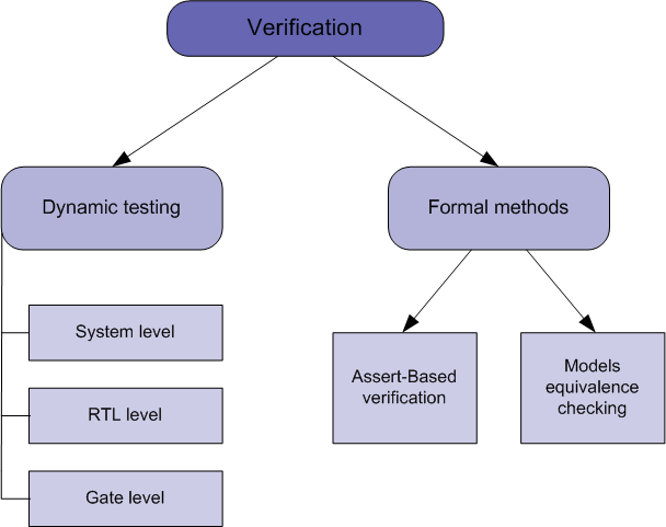
Fugure 3 — Main verification methods
Dynamic methods include simulation experiments on development project at various design levels — system level, RTL level, gate level. In each case test stimuluses are submitted to device inputs and the results are compared with the expected results. In this case device under test (DUT) can be a prototype or a model. A feature of the model and its compliance with the interim performance, and these factors combined can be controlled separately with this verification approach. The advantage of this method is the theoretical possibility of full coverage closure. In practice, it often happens that DUT is presented as a black box
and we can’t generate the stimuluses to test the full functionality. Also the number of test vectors for full coverage closure may be too large and lead to more time-consuming. Another disadvantage of this approach is the possibility of a situation when it’s impossible to observe the source of the internal circuits error. Such errors usually appear at later design levels. It leads to additional time and material costs.
Formal verification methods include the usage of the specifications of the project in his model, and different models equivalence evidence.
Methods of implementing the specifications of the project in its model are based on various properties of the project, which are controlled by the assertions within the project. Thus, the model of the project will contain a functional description and a description of properties monitoring. Methods of rigorous mathematical evidence provide that the model will have a planned future system properties [2]. These methods are called assertion methods. The simplest implementation of this method is the inclusion of assertions in the code, which control certain features of the project. This is achieved by applying a simple HDL-type assert operators, and by the usage of specific assertions describing languages — PSL (Property Specification Language), OVA (OpenVera Assertions) to describe the complex behavioral algorithms. The development of this methodic has led to methodology that based on the usage of assertions — ABD (Assertion-Based Design), which imlements the idea of assertion modules usage, for example, from Accellera OVL (Open Verification Library) library. The most important by assertions using is the right choice of monitoring properties of the object. With proper selection of the properties the completeness of coverage closure can reach a maximum.
The method of evidence the equivalence of models is based on a comparison of the current model with another (golden) model. This raises the problem of determining the correctness of the golden model. An example of using this method is the equivalence of RTL- and gate- representations comparing.
The advantage of formal methods usage is sufficiently large coverage closure in comparison with the dynamic methods when we have properly and complete selection of monitoring properties, as well as the ability to test the control points of the system. The disadvantage of these methods is the impossibility of their application at the level of the hardware implementation, as opposed to dynamic, which involve working with a prototype project; and also the complexity of CAD, which implementing formal verification methods. Comparative characteristics of verification methods speed performance [4] is shown on fig. 4.
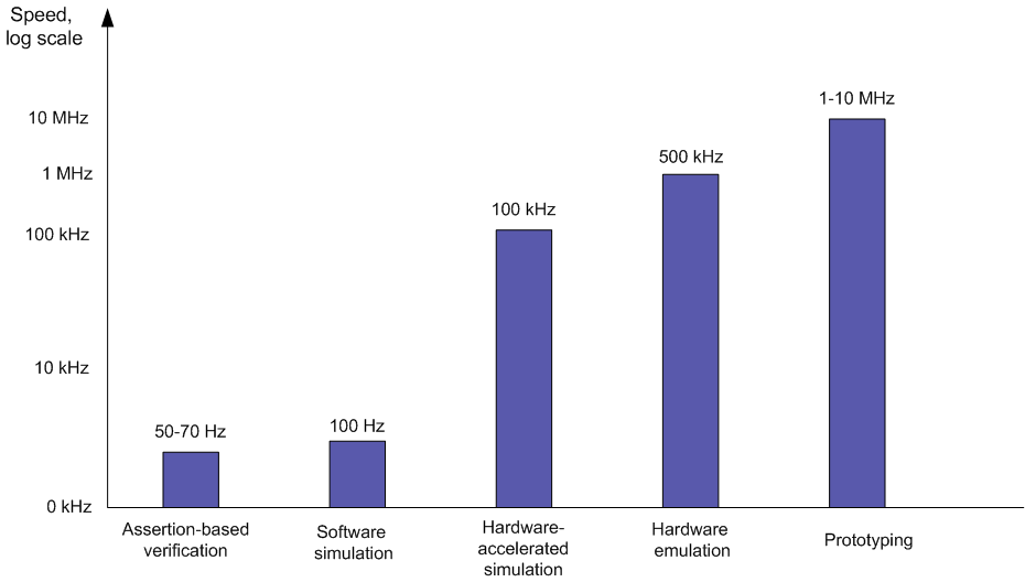
Figure 4 — Comparison of speed performance
Features of based on FPGA digital devices CAD design significantly reduce the cost of design errors. However, still remains an important time factor. Therefore, there is necessary to take into account the importance of more complete coverage closure at all levels of design with the use of existing verification methods and their combinations by design of complex devices, such as SoC. This entails the need to create a qualitatively new methodology for based on FPGA SoC verification, allowing for the target platform.
Development of a new methodology must solve the following problems:
- Reducing the time from initial design to the finished product;
- Maximizing coverage closure of verification;
- Exclusion of verification redundancy.
The FPGA-based SoC design/verification flow is shown on fig. 5.
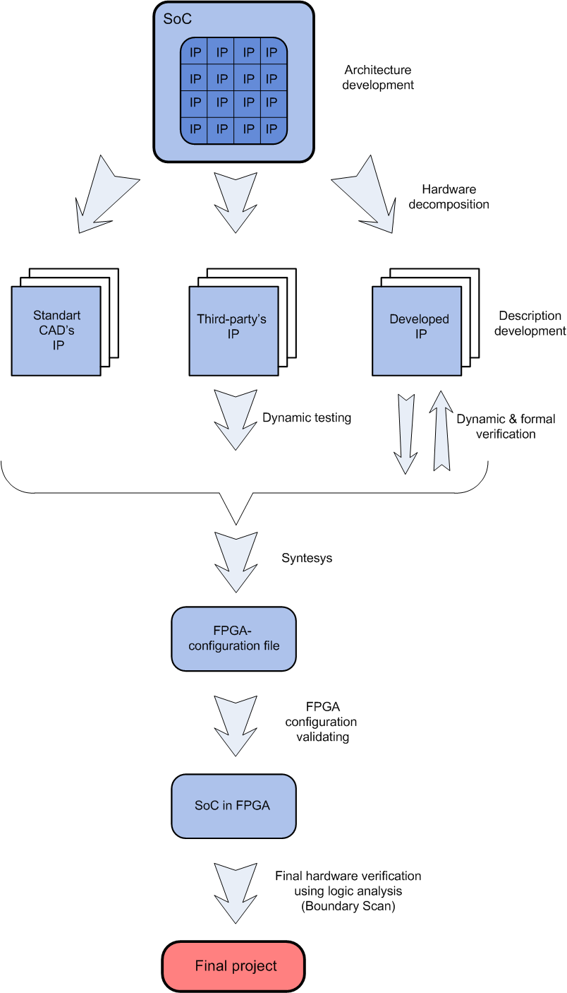
Figure 5 — Design/verification flow of SoC on FPGA
The means that must solve this problems are:
- Decomposition of SoC at the IP-core components, with the usage of individual verification methods;
- The right choice of verification methods and their usage at all levels of design, in contrast to the standard FPGA-based projects design flow of Xilinx company [5], where the verification procedure takes place only after the synthesis as a functional device simulation without verifying the basic description;
- The combination of top-down and through verification methods to ensure maximum coverage closure of the project;
- The usage of Boundary Scan technology to verify the authenticity of the crystal flash writing by reading back the configuration data from a programmed FPGA and compare with the contents of the programming file [6];
- The usage of Boundary Scan technology for dynamic hardware project verification by connecting the analyzing cores, for example, by using ChipScope Pro tools with standard algorithms for probe diagnostics.
Conclusion
Master's work is dedicated to actual scientific problem of usage the existing methods for digital devices verification for SoC on FPGA verification.
The review of existing methods of digital devices design has been found that deficiency of verification procedures at various levels of design and verification at the final stage often leads to additional material and time costs associated with the pullback in the early stages of development intended to correct errors. However, even small undetected logic error in the early design level can lead to total inoperability of a product after manufacturing of prototype.
For research the existing solutions on the application of verification methods at various levels of design to reduce overall design time and error detection in the early levels of development was carried out reviews of the most common present verification methods. The advantages and disadvantages of each method were identified, as well as their possible application areas.
It was decided to create a qualitatively new verification methodology for system-on-chip based on FPGA, allowing for the target platform, which should solve a number of issues. Minimizing the development time is still a pressing problem. A new methodology for the verification should be based on proper selection and usage of existing methods for each of the levels of designing individual and to ensure proper coverage closure of the project with the exclusion of coverage verification redundancy. The main mechanism here should be the use of Boundary Scan mechanism that would provide access to internal signals of the project for their control, which greatly enhance the ability of the dynamic verification and negate some of its shortcomings that limit its application.
This master's work is not completed yet. Final completion: December 2012. The full text of the work and materials on the topic can be obtained from the author or his scientific adviser after this date. The current state of research is displayed on a personal web site [7], dedicated to the problems of FPGA-projects verification.
References
- Немудров В., Мартин Г. Системы-на-кристалле. Проектирование и развитие [текст] / В. Немудров, Г. Мартин — М.: Техносфера. — 2004. — 216 с.
- Грушвицкий Р., Михайлов М. Проектирование в условиях временных ограничений: верификация проектов (1 часть) [Электронный ресурс]. — Режим доступа: http://www.kit−e.ru/assets/files/pdf/2008_3_96.pdf.
- Verification Horizons. A publication of Mentor Graphics — volume 8, issue 1 [Электронный ресурс]. — Режим доступа: http://www.mentor.com/products/fv/verificationhorizons/.
- Зотов В. Практический курс сквозного проектирования цифровых устройств на основе ПЛИС фирмы Xilinx (Часть 2) / В. Зотов // Современная электроника №2. — 2007. — с. 72-77.
- Зотов В. Практический курс сквозного проектирования цифровых устройств на основе ПЛИС фирмы Xilinx (Часть 20) / В. Зотов // Современная электроника №2. — 2009. — с. 48-55.
- Chong-Min Kyung Current Status and Challenges of SoC Verification for Embedded Systems Market — IEEE International SoC Conference [Электронный ресурс]. — Режим доступа: http://www.docstoc.com/docs/55759007/Current−Status−and−Challenges−of−SoC−Verification−for−Embedded.
- Верификация FPGA-проектов [Электронный ресурс]. — Режим доступа: https://sites.google.com/site/electricgorokhov/home.