Автор: Tony van Roon (VA3AVR)
Ссылка на источник: http://www.uoguelph.ca/~antoon/gadgets/pll/pll.htmlWhat Exactly is a PLL?

What Exactly is a PLL?
PLL stands for 'Phase-Locked Loop' and is basically a closed loop frequency control system, which functioning is based on the phase sensitive detection of phase difference between the input and output signals of the controlled oscillator (CO). You will find no formulas or other complex math within this tutorial. I decided to keep it simple.
But, before we go into any detail, first a little bit of history of the Phase-Locked Loop and prior to that with the superheterodyne.
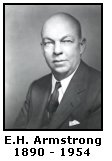
In the early 1930's, the superheterodyne receiver was king. Edwin Howard Armstrong is widely regarded as one of the foremost contributors to the field of radio-electronics. Among his principal contributions were regenerative feedback circuits, the superheterodyne radio receiver, and a frequency-modulation radio broadcasting system. It superseded the tuned radio frequency receiver TRF also invented by Armstrong in 1918. He was inducted into the National Inventors Hall of Fame in 1980. Armstrong was born on December 18, 1890, in New York City, where he was to spend much of his professional career. He graduated with a degree in electrical engineering from Columbia University in 1913, and observed the phenomenon of regenerative feedback in vacuum-tube circuits while still an undergraduate. At Columbia, he came under the influence of the legendary professor-inventor,
 Michael I. Pupin, who served as a role model for Armstrong and became an effective promoter of the young inventor. In 1915 Armstrong presented an influential paper on regenerative amplifiers and oscillators to the IRE. Subsequently, regenerative feedback was incorporated into a comprehensive engineering science developed by Harold Black, Harry Nyquist, Hendrik Bode, and others in the period between 1915 and 1940.
Armstrong conceived the superheterodyne radio receiver principle in 1918, while serving in the Army Signal Corps in France. He played a key role in the commercialization of the invention during the early 1920's. The Radio Corporation of America (RCA) used his superheterodyne patent to monopolize the market for this type of receiver until 1930. The superheterodyne eventually extended its domain far beyond commercial broadcast receivers and, for example, proved ideal for microwave radar receivers developed during World War II.
However, because of the number of tuned stages in a superheterodyne, a simpler method was desired. In 1932, a team of British scientists experimented with a method to surpass the superheterodyne. This new type receiver, called the homodyne and later renamed to synchrodyne, first consisted of a local oscillator, a mixer, and an audio amplifier. When the input signal and the local oscillator were mixed at the same phase and frequency, the output was an exact audio representation of the modulated carrier. Initial tests were encouraging, but the synchronous reception after a period of time became difficult due to the slight drift in frequency of the local oscillator. To counteract this frequency drift, the frequency of the local oscillator was compared with the input by a phase detector so that a correction voltage would be generated and fed back to the local oscillator, thus keeping it on frequency. This technique had worked for electronic servo systems, so why wouldn't it work with oscillators? This type of feedback circuit began the evolution of the Phase-Locked Loop.
As a matter of fact, in 1932 a scientist in France by the name of H.de Bellescise, already wrote a subject on the findings of PLL called "La Rйception Synchrone", published in Onde Electrique, volume 11. I guess he lacked the funding or did not know how to implement his findings. In either case it is my personal belief that the British scientist team developed further on the findings of Bellescise. No problem, good stuff. That's why papers like Bellescise are there for.
Although the synchronous, or homodyne, receiver was superior to the superheterodyne method, the cost of a phase-locked loop circuit outweighed its advantages. Because of this prohibitive cost the widespread use of this principle did not begin until the development of the monolithic integrated circuit and incorporation of complete phased-lock loop circuits in low-cost IC packages-- then things started to happen.
In the 1940s, the first widespread use of the phase-locked loop was in the synchronization of the horizontal and vertical sweep oscillators in television receivers to the transmitted sync pulses. Such circuits carried the names "Synchro-Lock" and "Synchro-Guide." Since that time, the electronic phase-locked loop principle has been extended to other applications. For example, radio telemetry data from satellites used narrow-band, phase-locked loop receivers to recover low-level signals in the presence of noise. Other applications now include AM and FM demodulators, FSK decoders, motor speed controls, Touch-Tone® decoders, light-coupled analog isolators, Robotics, and Radio Control transmitters and receivers. Nowadays our technology driven society would be at a loss without this technique; our cell phones and satellite tv's would be useless, well, actually they would not exist.
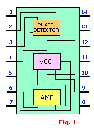
The PLL is a very interesting and useful building block available as a single integrated circuits from several well known manufacturers. It contains a phase detector, amplifier, and VCO, see Fig. 1 and represents a blend of digital and analog techniques all in one package. One of of its many applications and features is tone-decoding.
There has been traditionally some reluctance to use PLL's, partly because of the complexity of discrete PLL circuits and partly because of a feeling that they cannot be counted on to work reliably. With inexpensive and easy-to-use PLL's now widely available everywhere, that first barrier of acceptance has vanished. And with proper design and conservative application, the PLL is as reliable a circuit element as an op-amp or flip-flop.
Fig. 2 shows the classic configuration. The phase detector is a device that compares two input frequencies, generating an output that is a measure of their phase difference (if, for example, they differ in frequency, it gives a periodic output at the difference frequency). If fIN doesn't equal fVCO, the phase-error signal, after being filtered and amplified, causes the VCO frequency to deviate in the direction of fIN . If conditions are right, the VCO will quickly "lock" to fIN maintaining a fixed relationship with the input signal.
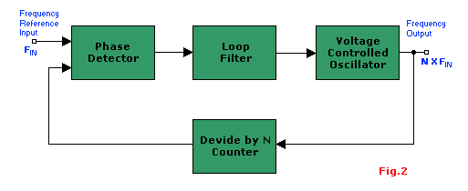
At that point the filtered output of the phase detector is a dc signal, and the control input to the VCO is a measure of the input frequency, with obvious applications to tone decoding (used in digital transmission over telephone lines) and FM detection. The VCO output is a locally generated frequency equal to fIN , thus providing a clean replica of fIN, which may itself be noisy. Since the VCO output can be a triangle wave, sine wave, or whatever, this provides a nice method of generating a sine wave, say, locked to a train of pulses. In one of the most common applications of PLLs, a modulo-n counter is hooked between the VCO output and the phase detector, thus generating a multiple of the input reference frequency fIN.
 This is an ideal method for generating clocking pulses at a multiple of the power-line frequency for integrating A/D converters (dual-slope, charge-balancing), in order to have infinite rejection of interference at the power-line frequency and its harmonics. It also provides the basic technique of frequency synthesizers.
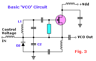
A basic Voltage Controlled Oscillator (VCO) can be seen in Fig. 3. It shows a basic voltage controlled oscillator by which frequency of oscillation is determined by L1, C2, and D2. D2 is a so-called varactor or varicap. Most common diodes will behave as a varicap when reversed biased, but they must be operated below the junction breakdown parameters.
With reverse bias, this diode will act as a capacitor, its depletion zone forming the dielectric properties. Changing the amount of reverse bias within the diode's breakdown limits, will alter the depletion zone width and hence vary the effective capacitance presented by the diode. This in turn changes the frequency resonancy of the oscillator circuit.
But how does this help us? After all, the VCO is not stable. Any slight voltage variation in the circuit will cause a shift in frequency. If there was some way we could combine the flexibility of the VCO with the stability of the crystal oscillator, we would have the ideal frequency synthesis system.
What if we feed the output of a VCO and Crystal Oscillator into a phase detector? What is a Phase Detector? (See Fig. 4). It is similar to a discriminator or ratio detector used in frequency demodulation or it could be a digital device, like an 'Exclusive OR' gate.
If two signals are fed into a phase detector, being equal in phase and frequency, there will be no output from the detector. However, if these signals are not in phase and frequency, the difference is converted to a DC output signal. The greater the frequency/phase difference in the two signals, the larger the output voltage.

Look at Fig. 4. The VCO and Crystal Oscillator outputs are combined with a phase detector and any difference will result in a DC voltage output. Suppose this DC voltage is fed back to the Voltage Control Oscillator in such a way that it drives the output of the VCO towards the Crystal Oscillator frequency--eventually the VCO will LOCK onto the crystal oscillator frequency. This phenomena is referred to as Phase Locked Loop in its most basic form. Only part of the VCO output needs to be sent to the phase detector. The rest can be usable output.
But hold on a minute, the VCO is locked onto the crystal oscillator and is therefore behaving as if it were a fixed frequency oscillator. This gives us the stability of a crystal oscillator, but lost the flexibility we were aiming for. We may just as well use the crystal oscillator alone for all the good this arrangement has done to us. It certainly doesn't appear as if we have accomplished anything at all.

Let's investigate how we can solve this problem. Suppose our crystal frequency was 10 MHz, but we wanted the VCO to operate on 20 MHz. The phase detector will of course detect a frequency difference and pull the VCO down to 10 MHz, but what if we could fool the phase detector into thinking the VCO was really only operating on 10 MHz, when in reality it is operating on 20 MHz. Take a look at Fig. 5. Suppose, for example in Fig. 4 we used a divide-by-four instead of the divide-by-two. Then, at LOCK, the VCO would be oscillating at 40 MHz yet still be as stable as the crystal reference frequency.
There are oscillators that will operate over a large range of frequencies. Variable Frequency Oscillators (VFO) are made to change frequency by changing the value of one of the frequency determining circuits. A VCI is one in which this component is made to change electronically.

PLL Components
Phase Detector: Let's have a look at the basic phase detector. There are actually two basic types, sometimes referred to as Type I, and Type II. The Type I phase detector is designed to be driven by analog signals or digital square-wave signals, whereas the Type II phase detector is driven by digital transitions (edges). They are typified by the most common used 565 (linear Type I) and the CMOS 4046, which contains both Type I and Type II.
The simplest phase detector is the Type I (digital), which is simply an Exclusive-OR gate (see Fig. 5a.). With low-pass filtering, the graph of the output voltage versus phase difference is as shown, for input square-waves of 50% duty-cycle. The Type I (linear) phase detector has similar output-voltage-versus-phase characteristics, although its internal circuitry is actually a "four-quadrant multiplier", also known as a "balanced mixer". Highly linear phase detectors of this type are essential for lock-in detection, which is a fine technique.
Todays engineers face constant challenges in the design of PLL circuits because of the level of phase noise and the fundamental property of noise floor signals, especially in the design of radio and wireless networks.
More recently, switching speed of PLL's have become a critical parameter in todays design of synthesizers, and especially for our modern networks such as 3G, WLANs, WCDMA, and Bluetooth technology. The switching speed is emerging as a challenging requirement for single loop, single chip PLL designs. Speed is mainly a function of loop bandwidth, but in many cases the loop band width cannot be too wide because of phase noise considerations. Speed-up techniques have been devised to improve PLL transient time, but most of them have limited efficiency.
In addition, speed-up techniques will have to be improved. For the WCDMA and 3G markets (and others emerging) a reasonable goal is 100 to 150mS for a dF=60Mhz excursion and a convergence to df=250Hz. One solution the industry will probably adopt in the future is the use of highly complex Sigma Delta fractional PLL architectures, which allow a high reference frequency and wide loop bandwidth, while maintaining resolution and a good phase noise profile (low division). This technique is already being implemented today.
Again, I can show you lots of formulas and all sorts of complicated equations but that would defeat the "easy-to-read" nature of my tutorials, including this one, so I pass on that and leave the math to others.

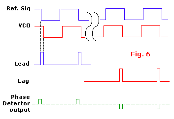
The type II phase detector is sensitive only to the relative timing of edges between the signal and VCO input, as shown in Fig. 6.. The phase comparator circuit generates either lead or lag output pulses, depending on whether the VCO output transitions occur before or after the transitions of the reference signal, respectively. The width of these pulses is equal to the time between the respective edges. The output circuitry then either sinks or sources current (respectively) during those pulses and is otherwise open-circuited, generating an average output-voltage-versus-phase difference like that in Fig. 7. This is completely independent of the duty cycle of the input signals, unlike the situation with the type I phase comparator discussed earlier. Another nice feature of this phase detector is the fact that the output pulses disappear entirely when the two signals are in lock. This means that there is no "ripple" present at the output to generate periodic phase modulation in the loop, as there is with the type I phase detector. Also, there is an additional difference between the two kinds phase detectors. The type I detector is always generating an output wave, which must then be filtered by the loop filter. Thus, in a PLL with type I phase detector, the loop filter acts as a low-pass filter, smoothing this full-swing logic-output signal. There will always be residual ripple, and consequent periodic phase variations, in such a loop. In circuits where phase-locked loops are used for frequency multiplication or synthesis, this adds "phase-modulation sidebands" to the output signal.
By contrast, the type II phase detector generates output pulses only when there is a phase error between the reference and the VCO signal. Since the phase detector output otherwise looks like an open circuit, the loop filter capacitor then acts as a voltage-storage device, holding the voltage that gives the right VCO frequency. If the reference signal moves away in frequency, the phase detector generates a train of short pulses, charging (or discharging) the capacitor to the new voltage needed to put the VCO back into lock.
The second-order PLL, serves as the basis for all PLL synthesizer designs and technology. Most PLL designs, especially for synthesizers where third and fourth order loops are common, use a different terminology, and deal mainly with the open loop gain and phase.
To name a couple of PLL devices from different manufacturers: NE560 to NE567 (Signetics), MC4046 COS/MOS (Motorola), LM565 (National), NTE989 (NTE Electronics).
General Features
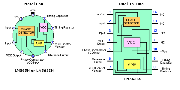
The LM565 is a general purpose Phase-Locked Loop IC containing a stable, highly linear voltage controlled oscillator (VCO) for low distortion FM demodulation, and a double balanced phase detector with good carrier suppression. The VCO frequency is set with an external resistor and capacitor, and a tuning range of 10:1 can be obtained with the same capacitor. The characteristics of the closed loop system--bandwidth, response speed, capture and pull in range--may be adjusted over a wide range with an external resistor and capacitor. The loop may be broken between the VCO and the phase detector for insertion of a digital frequency divider to obtain frequency multiplication.
A Phase-Locked Loop has basically three states:
- Free-running.
- Capture.
- Phase-lock.
The range over which the loop system will follow changes in the input frequency is called the lock range. On the other hand, the frequency range in which the loop acquires phase-lock is the capture range, and is never greater than the lock range.
A low-pass filter is used to control the dynamic characteristics of the phase-locked loop. If the difference between the input and vco frequencies is significantly large, the resultant signal is out of the capture range of the loop. Once the loop is phase-locked, the filter only limits the speed of the loop's ability to track changes in the input frequency. In addition, the loop filter provides a sort of short-term memory, ensuring a rapid recapture of the signal if the system is thrown out of lock by a noise transient. However, a design of a loop filter represents a compromise in that the parameters of that filter restrict the loop's capture range and speed, it would almost be impossible for the phase-locked loop to lock without it.
General Features and Applications
- 200ppm/°C frequency stability (drifting) of the VCO
- Power supply range of 5 to 12 volts with 100ppm/% typical
- 0.2% linearity of demodulated output
- Frequency range 0.001 Hz to 500 KHz
- Highly linear triangle wave output
- Linear triangular wave with in phase zero-crossings available
- TTL and DTL compatible phase detector input and square wave output
- Adjustable hold in range from 1% to more than 60%
Some Applications:
- Data and Tape Synchronization
- Modems
- FSK Modulation
- FM Demodulation
- Frequency Synthesizer
- Tone Decoding
- Frequency Multiplication and Division
- SCA Demodulators ('Hidden' Radio)
- Telemetry Receivers
- Signal Regeneration
- Coherent Demodulators
- Satellite
- Robotics & Radio Control

Check out the internal component diagram of the LM565 above.
This tutorial is pretty short in comparison with the 555 and 741 tutorials. Reason is that the complexity and relative complicity of the PLL is still being studied and the real possibilities just more and more realized. Peculiarities are, and will, still be discovered as time goes on. A couple of these to be noticed are the fact that in the case of 'ideal components within the PLL' there exists some systematic phase errors, in that the harmonic content of the output signal is of quite a complicated structure and that the wide band properties of the PLL are also not so simple a thing as it is sometimes taken discussing the matter. We are not done yet with this amazing device by a long shot, for many years to come.
In applications the PLL system is often used in combination with the Automatic Frequency Control (AFC) system and (or) automatic gain (signal level) control system.
Other Useful Applications Information
In designing with phase locked loops the important parameters of interest are:
- FREE RUNNING FREQUENCY:
- fo = 1/3.7 R0C0
LOOP GAIN:
The Loop Gain relates to the amount of phase change between the input signal and the VCO signal for a shift in input signal frequency (assuming the loop remains in lock). In servo theory, this is called the "velocity error coefficient".
- Loop gain = KoKD (1/sec)
- Ko = oscillator sensitivity (radians per sec/V)
- KD = phase detector sensitivity (V/radian)
The loop gain of the LM565 is dependent on supply voltage, and may be found from:
- KoKD = 33.6 fo/Vc
- fo = VCO frequency in Hz
- Vc = total supply voltage to circuit
Loop gain may be reduced by connecting a resistor between Pin 6 and Pin 7; this reduces the load impedance on the output amplifier and hence the loop gain.
HOLD IN RANGE:
The Hold In Range is the range of frequencies that the loop will remain after initially being locked.
- fH = ± 8 fo/Vc
- fo = VCO frequency in Hz
- Vc = total supply voltage to circuit
THE LOOP FILTER:
In almost all applications, it will be desirable to filter the signal at the output of the phase detector (Pin 7). A simple lag filter may be used for wide closed loop bandwidth applications such as modulation following where the frequency deviation of the carrier is fairly high (greater than 10%), or where wide-band modulation signals must be followed.
For narrow band applications where narrow noise bandwidth is desired, such as applications involving tracking a slowly varying carrier, a lead lag filter should be used. In general the damping factor for the loop becomes quite small resulting in large overshoot and possible instability in the transient response of the loop.
Abbreviations: AFC - Automatic Frequency ControlAM - Amplitude Modulation CCO - Current Controlled Oscillator CO - Controlled Oscillator COS - Carrier Operating System DTL - Diode-Transistor-Logic FC - Frequency Control FM - Frequency Modulation FSK - Frequency Shift Keying IC - Integrated Circuit OS - Operating System PLL - Phase-Lock Loop SCA - Subsidiary Communications Authorization (Hidden Radio) TTL - Transistor-Transistor-Logic VCO - Voltage Controlled Oscillator VCV - VCO Correction Voltage
To see an example of a working PLL doing its job, check out the circuit below of Fig. 8. This schematic diagram shows a so-called SCA adapter. The abbreviation "SCA" stands for Subsidiary Communications Authorization. It is used for 'hidden' messages, music, etc. on a normal hidden section of the FM band. It is based on a 67-KHz subcarrier that is placed on a station's main FM carrier. It is even possible to have multiple subcarriers, some carrying digital data, audio, data encryption, coded messages, and more. Subcarrier transmissions have no effect on standard FM mono and stereo bands and are fully compatible with all existing radios. This circuit can be hooked up to most fm tuners with a minimum of fuss. Low in cost, it uses just a few readily available IC's. The use of a Printed Circuit Board for this design is recommended.

Copyright and Credits
Some quotations are from the book: "The Art of Electronics", by Horowitz and Hill, listed below. SCA Adapter copyright by Hands-On Electronics(Jan. 1989) and Gernsback Publishing (No longer in business).
Suggested Reading on PLL Topics
"Design of Phase-Locked Loop Circuits". Howard M. Berlin. Publisher Sams. ISBN: 0-672-21545-3."Phase-Locked Loop Circuit Design". Dan H. Wolaver. Worcester Polytechnic Institute. ISBN: 0-13-662743-9
"Phaselock Loop". A. Blanchard. N.Y., John Wiley and Sons, 1976.
"Phase Locked Loops". Chapman & Hall, 1993. Original version: Systйmes б verrouillage de phase (P.L.L.) Masson, Paris, 1989
"Modern Communication Circuits". J. Smith. McGraw-Hill, 1986.
"Phase-Locked Loop: Design, Simulation, and applications". Donald E. Best, McGraw-Hill, 4th edition
"Phase-Locked Loops, Theory, Design and Applications". Roland Best. McGraw-Hill, NY 1984. ISBN: 0-07-911386-9.
"Synchronization System in Communications & Control". W.C.Lindsey. Englewood Hall NJ, Prentice hall, 1972.
"Digital PLL Frequency Synthesizers". Ulrich Rohde. Prentice-Hall, London, 1983.
"Digital Frequency Synthesis Demystified". B.G. Goldberg, LLH Publishing, 1999
"Phaselock Techniques". Floyd M. Gardner. John Wiley & Sons, New York, 1981, 2nd edition.
"Principles of Coherent Communication". McGraw-Hill, New York, 1966.
"La rйception Synchrone", Onde Electrique, volume 11, 1932. by H. de Bellescise.
"Phase-Locked Loop Basics". William Egan, Wiley InterScience, July 1998
"Frequency Synthesis". by V.F. Kroupa. Wiley, New York, 1973
"The Art of Electronics". Horowitz and Hill. 2nd Edition, 1989. Cambridge University Press. ISBN: 0-521-37095-7.