
Introduction
The device and principles of functioning of a random access memory.
The review of existing testing aids of storage
The analysis of a problem of testing of storage.
Algorithm of scoping of storage
Read SPD
Conclusions
References
Urgency
The considered task is a part of
architectural monitoring of productivity of the computer and is on
boundary hardware and the software.
Random access memory - one of the major elements of the computer. From
it the processor takes programs and the initial data for handling, in
it he writes down the received results. Random access memory
manufacture technologically difficult process. Complexity of
manufacture consists that the tendency on constant reduction of the
sizes of integrated circuits and increase of requirements to finished
goods prevails that in turn lifts requirements to materials of which
storage is made, being exposed to constant physical influence, it
should, for the durable time, save the properties. All it does
inevitable appearance of malfunctions in the made chips. At any batch
of ready chips always there is defined a spoilage percent, generally it
is traced on manufacture, however the part of unworkable chips gets on
the market what to do in that case. Failures in storage operation can
become the reason of loss of the valuable user information and a part
of system OS. A special case is incompatibility of units of storage of
different vendors among themselves or with motherboards.
At storage maintenance important precisely the nobility its valid
characteristics. The modern motherboards admit to adjust some
parameters the information about which is read out from units of
storage. It, first of all values таймингов which are stored in the
special storage SPD which is on the unit.
The system identifies storage units on Serial Presence Detect (SPD
protocol. SPD unit, is non-volatile chip EPROM (volume 256 byte) in
which the information on the storage unit, necessary for its correct
configuration contains: serial numbers of products and names of vendors
etc. BIOS reads out this data at start, and for initialization uses
them. The programs of diagnostics launched under OS read SPD. At
comparing of volume of the random access memory selected with OS and
BIOS with real capacity of installed units, it is possible to find out
a difference.
The named reasons testify that methods of a program estimation of
memory size, its allocations and as access to SPD is actual tasks in
creation of architectural basis of a specific platform of the personal
computer[9].
The
purposes and tasks
The operation purpose is algorithm elaboration тестирвоания storages,
and as development програмного supports on a basis разработаных
algorithms.
New tasks of this problem is creation of new test algorithms whose
эфективность should exceed existing analogs in times.
The primary goals which are subject to the decision:
1. The analysis of existing algorithms of testing of
storage.
2. Development of the concept of
new algorithms.
3.
Algorithm elaboration.
4.The software development, based on the developed
algorithms.
Random access memory — a part of system of computer storage by which the data and the commands necessary for the processor for performance of various operations are temporarily stored
Now in personal computers IBM PC storage of type DDR SDRAM is used, DDR SDRAM II and DDR SDRAM III.Аббревиатура SDRAM is decrypted as Synchronous Dynamic Random Access Memory — the synchronous dynamic memory with random access, DDR - Double Data Rate (double speed of data transfer).
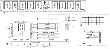
The general principle of the organization and functioning of chips of a dynamic memory (DRAM) is almost uniform for all its types — both initiating asynchronous, and modern synchronous. The storage array can be considered as a matrix (a two-dimensional array) elements, each of which contains one or several physical cells, capable to contain information elementary unit — one data bit. Cells represent a combination of the transistor (key) and the condenser (storage element). Access to matrix elements is carried out by means of decoders of the address of a line and the column address. From reasons of minimization of the size of package of a chip, the address of lines and columns are transferred on the same address lines of a chip. A singularity of storage of the given type is that condensers lose in due course the charge, for data loss prevention it is necessary to update contents of cells periodically. In the modern types of storage which support modes of automatic regeneration (in "the cleared" state) and itself regenerations (in "a sleeping" state), normally it is the task of the internal controler of the regeneration allocated immediately in a chip of storage. The schematic image of the unit of a random access memory is presented on fig. 1. One more singularity SDRA, the data array partition on some logical banks (at least — 2, it is normal — 4) is. The partition of an array of storage SDRAM on banks has been entered, mainly, from productivity reasons. Digit capacity of the data bus of the controler of storage and for all modern types of controlers of storage SDRAM (DDR, DDR2 and DDR3) makes 64 bits. Singularity SDRAM is one банковые ( single-rank) and two банковые ( dual-rank) units[8]. Two банковые storage units are most often presented by a configuration ";16 chips x8", thus one of physical banks (the first 8 chips) is allocated from unit face sheet, and the second of them (the remained 8 chips) — with back. More than one physical bank in the storage unit can't be considered presence as certain advantage since can demand magnification of time delays of the command interface.
Even
before appearance of the first type of the synchronous dynamic random
access memory SDR SDRAM by standard JEDEC it is provided that on each
unit of storage there should be the small specialized chip of ROM named
by a chip of "serial detection of presence" (Serial Presence
Detect, SPD). This chip contains the main information on type and a
configuration of the unit, temporal time delays which it is necessary
to adhere at performance of this or that operation at level of chips of
storage, and also the other information including the code of the
vendor of the unit, its serial number, manufacture date, etc.Scheme of interaction of memory with other PC components
depicted on Picture 2
Picture 1 – the
Schematic image of the unit of a random access memory (1); chips of
storage (2); matrixes (3) and separate storage cell (4).
Picture 2 – Scheme of interaction of memory with other PC components.
Memtest86 +.
This utility can be launched from the boot floppy disk or a compact disk. MemTest86 +, except the direct duties, defines the main characteristics of the computer, such as a chipset, the processor and speed of operation of storage. The program has two operation modes: basic and advanced (the main and expanded). They differ testing time. In the main mode it is possible to define any global problems with storage, and in an enhanced mode more careful testing is held.
Docmem - the random access memory Test.
Docmem is a convenient program for testing of storage which uses the deserved popularity. She can be rewritten from a site of vendors free of charge, only it is necessary to register. Program Docmem needs to be written down on a diskette with which help then it is necessary to load the computer. The program too offers two modes of testing: fast (quick) and the main (burn in) which is fulfilled, won't be stopped yet by the user.
Windows memory diagnostic - the random access memory Test.
The Microsoft company offers own diagnostic program similar to two previous. It is offered in the form of a standard installation file with image of a load compact disk and the program for creation load дискеты.Windows memory diagnostic is more simple program, than previous. Besides, it has additional test set for computer check. She allows to define, which unit is a source of problems if in system some units of storage are installed. To launch Memory Diagnostic, launch a file of the program and select that it is more convenient to you - to create a load compact disk or a diskette. At a choice of a compact disk you will ask where to save its image. Remember, where you have saved it, and use any program for record of CD of disks, for example, Nero.
If you select boot floppy disk creation (create startup disk) it is necessary to interpose simply into the disk drive a diskette and to wait, while on it the necessary information will be written down. After that will reboot, having loaded it by means of created a diskette or a compact disk.
The main lack of these programs is storage testing in a sparing mode. Despite продвинутость tests and a rich algorithmic dial-up, they can't reveal a problem, arising in modes, close to critical, therefore are situations in which all offered testers won't reveal errors, and during the maximum loading of the computer failures in random access memory operation start to happen. An output from the given situation is writing of own program of testing of storage.
Storage acceleration is rather radical means of performance improvement, but also extremely exacting to quality of units of storage. However, poor-quality units can сбоить even in a regular mode without any acceleration. Consequences of such errors are rather various: from abnormal termination of application before loss and-or distortion of the processed data.
Apparently, acquisition of "beaten" storage — at all a rarity and the people faces failures of storage regularly enough. To its immediate failure. More often defect is shown only at certain confluence of some circumstances. The heavy application "driving" storage "both in a tail, and in a mane", has every chance in a short space of time to "pick up" the necessary combination provoking failure.
Popular diagnostic programs, on the contrary, test rather restricted spectrum of modes in rather sparing conditions. Accordingly, and probability to find out an error in the latter case much more low.
Output — to Develop own testing program. At first, it is necessary to consider that the probability of failure is tightly connected to crystal temperature. The above temperature — the more possibly failure. And the temperature in turn depends on intensity of operation of storage. At the linear reading of cells the chip of storage at the expense of a batch mode is in time a little приостыть, maintaining in itself moderate temperature. Really, at request of one cell all DRAM-page is read entirely, being saved in internal buffers and until the following page of the same bank will be requested, no calls to a storage kernel happen!
Therefore, before to start real testing, storage is necessary for warming up properly, reading it with the step equal to length of DRAM-bank, it will force a kernel of the given bank to work as much as possible intensively, on each step fulfilling procedure of reading and recovering data record. It is not necessary to test some banks simultaneously. At first, it will lower temperature of "heat" of each of them, and, secondly, overfall of temperatures in a crystal increases probability of detection of failure a little.
When the storage unit has heated up so that won't be retained by a hand, it is a high time to start the present tests. We fill DRAM-page with control sequence of numbers (further under the text — a template), we switch page that гарантированно to update storage cells (otherwise a chip can return contents of the buffers, without addressing to a memory matrix). Again we switch page back and we check that we have written down.
Rather rigid demands are made to a template. At first, it should test each bit of a cell, and, for both values — unit and a zero as "beaten" cells of a matrix can give or "always a zero", or "always unit". Secondly, it is extremely desirable, that in восьмерном a word adjacent bits had opposite values. Such combination creates the greatest interference level and by that provokes system to an error. Thirdly, the template should provide detection of address errors, i.e. situations when the chip has returned the cell content not that line and-or a column. As all these requirements mutually exclusive, for testing some templates is required. Only don't forget to fulfill from time to time "idle" reading for maintenance of temperature of a chip at as much as possible achievable level, differently efficiency of the test will start to fall.
Let's consider search of pages. Serial search, then — chaotic calls to pages on a casual template. However it is not enough of it, the modern controlers of storage independently define the preferable order of request processing, having analyzed algorithm, it can produce the buffer content, instead of real value.
For bypass of the mechanism of buffering необъодимо to check cells not right after record, and after a while when internal буферы the controler гарантированно will be superimposed by the subsequent requests. Same allows to reveal regeneration errors when because of any defects the charge from a matrix cell refluxs earlier, than it have time to recycle.
The developed algorithm of the program implements functions scoping of the installed storage, obtaining of a card random access memory allocation, reading of contents of chip SPD.
Random access memory scoping is fulfilled by means of interruption BOIS int 15h ax=E810h [2]. It allows to define volume of the installed storage to 4Гб. Interruption returns in register AX an amount 64 кб. Units between 1 and 16 mbytes of the installed storage, in register BX an amount 64кб. Units between 16мб. And 4гб. The installed storage, считав value of these registers we define volume of the installed random access memory.
Obtaining of a card allocation of address space of the installed storage it is executable by means of interruption BIOS int 15h AX=E820h. It allows to form the allocation map of address space of a random access memory. As input parameters the pointer is transferred to the buffer in register ES:DI, buffer volume in register ECX, EBX, for the first call is equal “0”, for the subsequent calls in EBX there will be an address of a following memory unit which will be returned before a going call of interruption. After a successful call of interruption in the buffer the value, storages characterizing a considered section are returned. [3] structure of the returned data is resulted in table 1.
Table 1. Structure of the returned data
| Offset | name | Description |
| 0 | BaseAddrLow | Low 32 Bits of Base Address |
| 4 | BaseAddrHigh | High 32 Bits of Base Address |
| 8 | LengthLow | Low 32 Bits of Length in Bytes |
| 12 | LengthHigh | High 32 Bits of Length in Bytes |
| 16 | Type | Address type of this range |
Field Typе defines possible types of storage, its structure is resulted in table 2.
Table 2. Structure of field Typе.
| Value | Description |
| 1 | AddressRangeMemory, available to OS |
| 2 | AddressRangeReserved, not available to OS |
| 3 | AddressRangeACPI, available to OS |
| 4 | AddressRangeNVS,not available to OS |
The call of the given interruption is
fulfilled in a cycle while value of register EBX won't be equal
“0”.
Any modern unit of storage can't do without a component — chips SPD (Serial Presence Detect). The interface of serial detection regulated at present for all units of storage of form factor SIMM/DIMM/RIMM, uses the control bus system (SMBus — System Management Bus), compatible to specification Inter-IC (I2C or IIC). The principle of usage of bus SMBus in case of SPD is reduced to data transfer from chip EEPROM.
For access to SPD it is necessary to use configuration registers of bus SMBus which are in configuration space PCI[10].
Configuration address space PCI consists from 256 byte which it is possible to address, knowing bus PCI number, number of the device and function number in the device. The first 64 bytes from 256 are standardized, and remaining registers can be used at the discretion of the manufacturer of the device.
Access to PCI through ports I/O. For operation with bus PCI in PC AT and compatible machines it is selected two main ports:
-0CF8h-W Address address port.
-0CFCh RW port of data Data.
Both ports are 32 bit. The address port represents the following 32 bit structure which sets the bus, devices, and the register address in a configuration device space. The structure of port of the address is resulted in table 3.
Table 3. Address port.
| 31 | 30.....24 | 23.....16 | 14....11 | 10....8 | 7....2 | 1 | 0 |
| C | Reserve |
Bus | Device | Function | Index |
In this structure the device is physically present device
where function is a logic device. With - an access flag to the device.
Low two bits in address port always 0. Upon termination of operation
with the device it is necessary to drop the address in 0.
The first step in access to chip SDP is creation of list PCI of
devices, by serial search of all possible PCI addresses and request of
reading of the zero register. If in reply to request of the zero
register it is returned 0FFFFh devices don't exist. If the device
exists we remember its address in the list of devices.
The second step is bus SMBus search in received list PCI of devices.
Search is carried out by inquiry of each address from list PCI of
devices and check of contents of configuration registers, for the
purpose of search by sign SMBus of the bus [4].
The third step. If bus SMBus is found in a case, we select one of
possible SDP addresses (50h, 51h, 52h, 53h) then of 256 byte in the
buffer, since the current address is executable byte-serial reading.
Following stage is interaction with controler SMBus through its range
of input/output ports. Base address SMB_Base. We nullify status bits in
register Host Status (SMB_Base+0) for preparation of the controler for
the next operation. Bits of this register use discipline Read/Write
Clear, and are nullified at record "1" in them.
We send a 8-bit cell address of chip SPD which is required to be read.
It registers in register Host Command (SMB_Base+3). At transaction
performance on bus SMBus, value of this register is transferred in the
field Command.
We transfer the 8-bit address of chip SPD to which reversal is
fulfilled. It registers in register Transmit Slave Address
(SMB_Base+4). At transaction performance on bus SMBus, value of this
register is transferred in the field Slave Address.
We launch the transaction performance which parameters have been
prepared. For this purpose it is necessary to write down the operation
code in register Host Control (SMB_Base+2). For start of operation of
transmission of byte the code 01001000b = 48h is used.
Controler SMBus begins read operation of byte from SPD. The program
should expect operation end. We interrogate a state of bit Host Busy,
it is bit 0 registers Host Status (SMB_Base+0). On value Host Busy=1 we
define the moment of the beginning of operation, then it is expected
Host Busy=0, that is operation completions. Absence of expected event
during the given interval (about 50 msec) is interpreted as an error
– таймаут buses.
We read out from register Host Data 0 (SMB_Base+5) the byte read
from SPD. Its value is authentic only in the absence of errors.
We check absence of errors. For this purpose we read out register
Host Status (SMB_Base+0) and it is analysable status bits. After
successful end of transaction, the state of bits 4-1 should be 0001b.
We mask the specified bit field and it is checked its value.
Having received 256 byte it is checked their value if all bytes are
equal FF SPD to the given address it is inaccessible. If SPD is
present, we make the analysis of bits interesting us from считаного the
buffer. The result of operation of the program,developed by the master Khachaturov, is presented in a
picture 3.
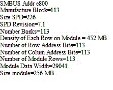
Picture 3. A fragment of
result of operation of the program. Bus address SMBus and contents SPD.
Program testing has shown that it successfully fulfills tasks in view: scoping of the random access memory installed on the computer, creation of the allocation map of storage, reading of chip SPD. The access method to SDP, considered in given article has singularities connected with implementation of bus access SMBus is various on different chipsets. The developed program can be used by development of operating systems “from zero”, to development of the specialized software for diagnostics as can be launched on partially serviceable system and fulfills the functions, at debugging of process of interaction of functions of the program with equipment.
Scientific innovation
Scientific novelty of the work is to develop an algorithm memory test, which will be based on the method of heating as well as in the proof of the effectiveness of the new algorithm can detect, in contrast to the previously existing algorithms,
failure of memory, which appear under extreme operating conditions of memory.
The developed algorithms are also distinguished by the fact that they have a small resource-intensive.
1. OSDev Wiki [Electronic resource]/ Internet resource. – Access mode : www/URL : http://ru.osdev.wikia.com/wiki/ Карта_ распределения_ памяти
2. INTERRUPT LIST [Electronic resource]/ Internet resource . – Access mode : www/URL : http://www.ctyme.com/intr/rb-1739.htm
3.INTERRUPT LIST [Electronic resource]/ Internet resource с . –Access mode: www/URL : http://www.ctyme.com/intr/rb-1741.htm
4. SMBus [ Electronic resource ]/ Internet resourceс. –Access mode: www / URL http://smbus.org/
5. JEDEC [ Electronic resource ]/ ИInternet resource. –Access mode: www / URL : http://www.jedec.org/
6.
M.Guk. Hardware IBM
PC. The encyclopedia. [Text] / M.Guk//"Peter" 2008.-C.1072.
7. INTEL [ Electronic resource ]/ Internet resourceс . –Access mode: www / URL http://www.intel.com/index.htm?ru_RU_05
8. CITFORUM [Electronic resource]/ Internet resourceс. –Access mode: www/URL : http://citforum.ru/book/optimize/ram.shtml
9. Lipworld [Electronic resource]/ Интернет-ресурс. –Режим доступа: www/URL : http://www.lipworld.by.ru/Lipworld_Text/zelezo/ozu/vvedenie.html
10. Wikipedia [Electronic resource]/ Интернет-ресурс. –Режим доступа: www/URL : http://en.wikipedia.org/wiki/Serial_presence_detect