Источник:http://www.techonline.com/article/pdf/showPDF.jhtml?id=2022016311
A New PLL Based Frequency Synthesis Technique
Kostas Efstathiou, El. Eng. Ph.D.
efstathiou@ee.upatras.gr
Applied Electronics Laboratory
Department of Electrical Engineering & Computer Technology
University of Patras
University Campus of Rio
26500 Patras, Greece.
Abstract
A new PLL based frequency synthesis technique is presented in
this paper. The new technique is able to sample the phase of
the reference and the output frequency at very high rate, in
contrast to the conventional PLL based synthesizer that samples
the phases of the two frequencies at a rate equal to the step
frequency. The increased sampling rate of the phases, results
to the increased convergence speed, and on the same time, to
the elimination of the spurs nearby the output frequency. The
resolution of the synthesizer can be significantly increased,
without limiting the settling time and without affecting the
quality of the output. Moreover, the behavior of the loop does
not depended any more from the output frequency.
1. Introduction
The designer of the PLL based frequency synthesizer has to compromise
the settling time, the resolution and the quality of the synthesized
frequency. The main reason for this design trade- offs is the
low sampling rate of the phase difference that is usually equal
to the step frequency of the synthesizer. As the requirement
for resolution increased, the sampling rate of the phase difference
decreased, resulting to the above mentioned trade offs.
Several techniques have been developed to increase the performance
of the PLL based synthesizer. As most popular can be considered
the Fractional-N techniques [1], [2], [3], which however, cannot
comply with the increased demands of the modern telecommunications.
The Digital Direct Frequency synthesizers are used instead, on
the penalty of the increased power consumption and the use of
up-converters required to synthesize high frequencies.
In this paper we present a technique that breaks through the
limitations of the conventional PLL based synthesizer. Applying
this technique, the phase of the reference and the output frequency
is sampled at very high rate and on the same time each phase
is normalized and their difference is calculated. The high sampling
rate of the phases of the two frequencies increases significantly
the performance of the synthesizer that becomes comparable to
this of the Digital Direct Frequency Synthesizer.
2. The Dual Input Phase Accumulator
According to the new technique, the Phase Frequency Detector
(PFD) and the dividers of the reference and the output frequency
of the synthesizer used in the conventional PLL based synthesizer,
are substituted with a DUAL INPUT PHASE ACCUMULATOR (DIPA) [4].
Inputs to the DIPA are the two frequencies of the synthesizer
(the reference and the output frequency) and two variables that
normalize the phases of the two input frequencies and correspond
to the numbers loaded to the dividers of the conventional synthesizer.
The DIPA operates according the following rule:
At each period of the Reference Frequency, a value proportional
to the Output Frequency is added to the accumulator, and at
each period of the Output Frequency, a value proportional to
the Reference Frequency is subtracted from the accumulator.
According to the rule the phase of each frequency is sampled
every 360°(2π) and therefore, the sampling rate of the
phase of each frequency is equal to the frequency itself.
2.1. The DIPA output
Let us examine the properties of the output of the DIPA assuming
that the Reference Frequency (Fref) is 5 and the Output Frequency
(Fout) is 7. According to the DIPA rule, the Reference Variable
(Vref) should be 7 and the Output Variable (Vout) should be 5.
The output of the DIPA and the phases of the two frequencies
are depicted in Fig. 1.
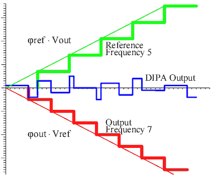
Figure 1. The output of the DIPA
The output of the DIPA due to the reference frequency is an
up going staircase with a step- width equal to the period of
the Reference Frequency and a step-height equal to the variable
Vout. Consequently, the output of the DIPA due to the output
frequency is a down going staircase with the corresponding characteristics.
Each staircase can be analyzed in two components:
- a ramp, with a slope proportional to the product of the phase
of the frequency and the corresponding variable
- and a sawtooth waveform of the frequency that generates
the staircase and an amplitude proportional to the corresponding
variable
The subtraction of the two ramps is the phase difference of
the normalized phases, while the subtraction of the two sawtooth
waveforms can be considered as the noise due the sampling of
the two phases. Thus, the output noise of the DIPA is derived
by the subtraction of the two sawtooth waveforms as is depicted
in Fig. 2. The sawtooth waveform has harmonics of the fundamental
frequency. Therefore, the output noise of the DIPA consists of
harmonics of the two high input frequencies, the reference frequency
and the output frequency.
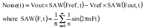
The filter of the loop has to reject these high frequencies,
while the filter of the conventional synthesizer has to reject
a low frequency, which is equal to the step frequency (Fstep)
of the synthesizer. In most of the cases the step frequency is
several thousand times lower than the reference and the output
frequency. Therefore the bandwidth of the LPF can be increased
significantly, increasing on the same time the bandwidth of the
loop.
Additionally it should be mentioned, that since the DIPA output
noise consists of high frequencies, it may required no filtering,
since this noise will appear very far from the synthesized frequency,
probably out of the useful band.
Figure 2. The DIPA's output noise
3. The Implementation of the DIPA
An implementation of the DIPA using digital technology can be
found at [5]. The hardware requirements for the digital implementation
do not demand a large amount of gates. A 16 bits DIPA has been
implemented on a 2.5 thousands gates, low cost FPGA. The results
derived by this implementation demonstrate the significant enhancements
of the DIPA based FS. However the DIPA is able to be implemented
using analog electronics.
The analog implementation of the DIPA is more attractive and
challenging than the digital one, since it consumes less power,
it can operate at higher frequencies, and requires significantly
less circuitry. However the analog implementation suffers from
the frequency error introduced by the imperfections of the analog
components used.
The first approach of the analog DIPA [6] proves that the frequency
error introduced due to the above-mentioned imperfections may
not be significant. In this paper we propose an alternative analog
implementation and we consider on the frequency error that introduces.
3.1. The analog DIPA
In Fig. 3 the analog DIPA is depicted. As it can be seen the
Analog DIPA consists of two identical blocks and a current mirror.
Each block consists of an Operational Amplifier, a voltage controlled
current source and its current mirror, and a Frequency Depended
Resistor (FDR). The Operational Amplifier controls the current
source so as to keep the voltage applied on the FDR equal to
its positive input. The current supplied to the FDR is measured
by the mirror of the current source. The currents derived from
the two blocks are subtracted with the aim of the middle current
mirror. The use of the capacitor Co integrates the difference
of the two currents.
Figure 3. The Analog DIPA
Each FDR is a CMOS inverter with a small capacitor C at its
output. The current flow through this inverter is depended on
the supply voltage of the inverter, the frequency that it toggles
and the capacitor. Thus, we can write the expression of the output
of the DIPA. It can be seen that the output of the DIPA is proportional
to the normalized phase difference of the two input frequencies.
Before studying the frequency error that introduces the DIPA,
due to the use of non-ideal components, we have to study the
behavior of a frequency synthesizer based on the ideal DIPA.
3.1.1 The DIPA in Blocks
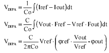
Let us assign the gain of phase detector as Kd and the Voltage
Ratio Vout over Vref as Kf.
According to the equation of the DIPA, it incorporates a multiplier
that multiplies the reference phase with the value Kf and an
adder with gain Kd (given in volts per radius) that calculates
the normalized phase difference. The block diagram of the DIPA
is given in Fig. 4.
Figure 4. The DIPA in Blocks
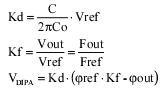
3.1.2 The DIPA Based Synthesizer
The DIPA based synthesizer, depicted in Fig. 5, incorporates
a Low Pass Filter (LPF) with a transfer function F(s) that rejects
the DIPA’s noise, the VCO and of course the DIPA. Optionally,
a prescaler may by used so as to scale the frequency of the VCO,
down to a frequency that the DIPA can handle.
Figure 5. The DIPA based frequency synthesizer
It should be emphasized that the feedback of the loop is always
constant and does not depended on the desired output frequency,
as it does in the conventional FS. Therefore, the designer does
not have to face any trade-off related to the behaviour of the
loop and depending on the frequency range that the FS has to
cover.
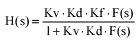
Assuming that the LPF is a lag filter, the parameters that control
the behaviour of the loop are given:
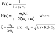
The second significant improvement of the frequency synthesizer
based on the DIPA is, that the Low Pass Filter (LPF) of the loop,
has to filter-out very high frequencies. Actually, it has to
filter out the reference and the output frequency. Therefore,
the designer is able to increase the bandwidth of the LPF and
consequently the bandwidth of the loop, by a value equal to the
ratio of the reference or the output frequency over the step
frequency of the synthesizer. In conventional PLL based Frequency
Synthesizer, this ratio is a number expressed in thousands. Thus,
the bandwidth of the loop can be increased several thousands
times. This, results to the increment of the convergence speed
of the loop at the same value. Moreover, the increased bandwidth
of the loop reduces significantly the phase noise of the synthesized
frequency at a wide frequency range. Additionally, it should
be emphasized that the output of the DIPA has not low frequency
components related to the step frequency of the synthesizer.
Thus, the spectrum nearby the synthesized frequency is clear.
Finally, the third significant improvement of the frequency
synthesizer based on the DIPA is, that the increased resolution
of the synthesized frequency does not affect the behaviour of
the loop. The step frequency of the synthesizer is depended on
the resolution of the variable Kf. Therefore the designer is
able to increase the resolution of the synthesizer with out to
worry about the convergence speed of the loop. Since Vout and
Vref are voltages, it is able to achieve even linear resolution.
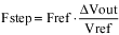
The step frequency of the synthesizer is:
3.2 The Accuracy of the Analog DIPA based FS
The limited gain of the OpAmp affects the precision of the voltage
applied on the FDR and consequently the accuracy of the synthesized
frequency. In order to increase the accuracy of the synthesized
frequency the OpAmps employed should have high gain and their
gain should be matched.
This can be easily achieved if the OpAmps are build-in the same
chip. However this requirement can be considered as a non-critical
requirement, since the frequency error that introduces is not
significant. For example, when the OpAmps have a gain of about
10.000 that is matched within 2%, they introduce a frequency
error that is less than 2 parts per million (PPM).
The frequency error introduced due to the DC Offset of the OpAmps
is critical. It is probably the most significant problem of the
analog DIPA.
Therefore, it is mandatory to use OpAmps with very low DC offset
and additionally we have to apply DC Offset cancellation techniques.
However it should be emphasized that this error is reduced as
the reference over the output frequency ratio is closed to one.
3.2.2 Imperfections of the FDR
The FDR is a CMOS inverter that drives a capacitor. The current
flows through the inverter should be equal to the current required
to charge the capacitor. During the transition of the input,
both MOSFETs of the inverter are on and a current flows through
the MOSFETs to the ground. In order to eliminate this current
we have to use the well known ‘Two Phase Clock Generator’ based
on the NOR latch and depicted in Fig. 6.
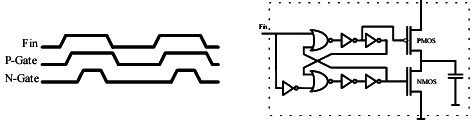
Figure 6. The FDR using a Two Phase Clock Generator
In order to eliminate further the FDR non-linearity, we use
two FDRs, as is depicted in Fig. 7, where the first one drives,
for example, a 2 pico-farads capacitor and the second one an
1 pico-farad capacitor. The current flow through the two FDRs
consists of the current required to charge the capacitor and
the current that introduces the non-linearity of the inverter.
Subtracting the currents flow through the two FDS, the non-linear
component is eliminated and remains the current required to charge
a capacitor equal to the difference of the two capacitors used.
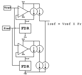
Figure 7. The FDR 'Compensation'
It has been found by simulations that the FDR with this type
of ‘compensation’ introduces frequency error that can be as small
as 50 parts per million over a wide frequency range. It also
has been found this error decreases, as the size of the MOSFETs
decreased and the difference of the two capacitors decreased.
It should be emphasized that the FDR compensation is not mandatory
when the ratio of the Reference over the Output frequency is
close to one. The frequency error introduced in this case is
negligible, since both FDRs have the about the same non-linearity.
4. Conclusions
The DIPA based Frequency Synthesizer and considerations on its
analog implementation have been presented in this paper. It is
apparent that the DIPA based synthesizer has a significantly
enhanced performance. More specifically:
- The settling time can be extremely small.
- The resolution can be even linear.
- There are no spurs near by the synthesized frequency.
- The behavior of the loop is not depended on the synthesized
frequency.
- and the phase noise is suppressed over a wide frequency range.
Obviously, the performance of the DIPA based synthesizer is
superior and it is not fair to compare it with this of the conventional
one.
The digital implementation of the DIPA does not suffer from
the imperfection of the devices used. The synthesized frequency
using the digital DIPA is extremely accurate, since the accuracy
is only depended on a ratio of two digital words representing
the variables Vout and Vref. The analog implementation is more
attractive, however the imperfections of the analog devices employed
for this implementation introduce a frequency error. More specifically
the analog DIPA:
- is simple and can be implemented easily on a chip
- can operate at high frequencies
- has low power dissipation
- but it suffers from the Frequency Error.
- and requires very careful design and manufacturing
It is estimated that in short time and with the aim of the advanced
IC technology, it will be able to obtain a very fast, very accurate
analog DIPA. Therefore, we can foretell that the analog DIPA
will become soon, the dominant frequency synthesis technique.
References
- Gillette G. C., 1969, The Digiphase principle. Frequency
Technology, Aug 1969, pp. 25- 29.
- Wheatley E. Charles, 1983, Digital Frequency Synthesizer
with random Jittering for reducing discreet spectral spurs.
United State Patent No. 4,410,954.
- Riley, Tom A.D.; Copeland, Miles A.; Kwasniewski, Tad A.
1993. Delta-Sigma modulation in fractional-n frequency synthesis.
IEEE Journal of Solid-State Circuits. 28 No. 5, pp. 553-559.
- K. A. Efstathiou, A., G. D. Papadopoulos, G. Kalivas, High
Speed Frequency Synthesizer based on PLL, IEEE International
Conference on Electronics, Circuits and Systems, Rodos, Oct.
1996, Vol. 2, pp. 627-630
- K. A. Efstathiou, G. D. Papadopoulos, "Implementation of
a High Speed Frequency Synthesizer employing a Dual Input Phase
Accumulator", International Journal of Electronics, pp. 43-56,
No. 1 Vol. 87, January 2000.
- K. A. Efstathiou, A., G. D. Papadopoulos, "An Enhanced Frequency
Synthesizer using an Analog Dual Input Phase Accumulator",
Proceedings of the Sixth IEEE International Conference on Electronics,
Circuits and Systems, Vol. 1, pp.17-20, Paphos, Cyprus, Sept.
1999.
|