Источник:www.radio-labs.com/DesignFile/dn005.pdf
Charge Pump saturation effects in PLL Frequency Synthesizers
Introduction
The PLL frequency synthesizer has become one of the basic building
blocks in modern communications systems. Many monolithic PLL
integrated circuits are available, which incorporate the needed
frequency dividers and the phase detector. An extremely common
phase detector is the charge pump.
It is common practice to use a charge pump phase detector with
a passive loop filter such as that shown in Figure 1
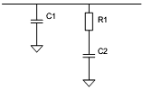
Figure 1. The Passive Loop Filter
In this configuration the voltage swing available to the VCO
is limited to the voltage supplied to the charge pump phase detector.
Typical integrated circuit operating voltages have resulted in
a 0 to 5V range being commonly available. As chip operating voltages
have been decreasing, there are options to reduce this voltage
range. This paper describes the detrimental effects on locking
performance if the charge pump voltage supply is decreased too
far.
Design Example
We will firstly illustrate the problem.
Consider a PLL designed for:
- Output frequency range: 100MHz to 130MHz
- Channel Spacing: 25kHz
- Charge pump current: 1mA
- VCO Kv = 10MHz/V
To centre the VCO range, assume that the VCO tunes from 90MHz
at 0V to 140MHz at 5V.
Loop bandwidth = 2.5kHz, Phase margin = 45 degrees C1 = 3.68nF,
R1 = 8.65k, C2 = 17.8nF
The transient response for a frequency step from the bottom
of the band to the top of the band is shown in Figure 2 where
it is assumed that the charge pump has unlimited voltage swing.
The lock time to within 1kHz is 1.21ms.
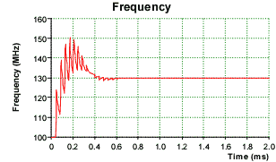
Figure 2. 100MHz to 130MHz Transient — no
limiting
The simulation in Figure 2 (and all others in this paper) were
performed using Applied Radio Labs SimPLL software package [1].
If we now introduce saturation in the charge pump output, where
we assume that the charge pump cannot deliver charge above 5V
or below 0V, the transient response becomes as shown in Figure
3:
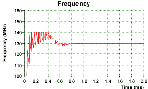
Figure 3. Limiting at 0V and 5V
The lock time to 1kHz has increased to 1.38ms. Reducing the
upper limiting voltage to 4.5V further increases the lock time
to 1.69ms with transient response shown in Figure 4
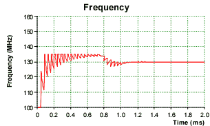
Figure 4. Limiting at 0.5V and 4.5V
To summarize:
| Clipping Level(Volts) |
Time to Lock to 1kHz (ms) |
| None |
1.21 |
| 5 |
1.38 |
| 4.5 |
1.69 |
| 4.25 |
2.21 |
Note that in each case the target steady state voltage on the
VCO control line is 4V.
So it can be seen that failing to provide adequate headroom
in the charge pump output can lead to significant increases in
PLL lock times. It also indicates that normal production variations
in VCO tuning law can lead to significant variations in PLL lock
time.
Discussion of effect
The reason for this effect may be readily understood from the
loop filter schematic Figure 1 and the unclipped transient in
Figure 2. Expanding the early part of the transient we see
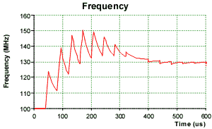
Figure 5. Expanded transient, no saturation
In the loop filter in Figure 1, C1≈0.1C2
At the beginning of the transient, the charge pump supplies
current to the loop filter to increase the VCO voltage. During
the short phase detector pulses this current flows primarily
into C1, (the voltage spikes) and in-between the spikes
much of the charge from C1 flows through R1 to
C2 (the decaying voltage between the spikes). To get
a reasonable current flow into C2 (which is the biggest)
necessarily requires the voltage across C1 to rise
to levels significantly above the voltage across C2.
Limiting these spikes significantly reduces the flow of current
into C2.
Conclusion
The voltage headroom provided at by the charge pump phase detector
can have significant effect on PLL lock time. The lack of sufficient
headroom can result in a major degradation of locking performance.
The effect on lock times can be readily determined using a simulation
package such as SimPLL.
References
- SimPLL software package, available at: www.radiolab.com.au (note
all simulations in this article can be performed using the
free demo version of SimPLL)
|