|
Swift development of the digital systems of commutation and facilities of passing to information resulted in considerable growth of role of the systems of synchronization in the networks of telecommunication. In digital hierarchical networks of data-transmission, both synchronous and asynchronous, in accordance with recommendations of ITU-T, and also ETSI (European telecommunication standards institute) is used the forced method of node synchronization. Because the synchronous mode allows more effectively to use the chains of data communication. An actual rate of transmission data in the asynchronous mode is 0,8 from declared. In the synchronous mode these speeds are identical, because only useful bits are passed.
The basic task of network synchronization is limitation of skips and slips. The signal of synchronization, arriving at a node, suffers from changes which can negatively tell on the process of synchronization.
In most cases for the selection of clock signal, which is transfered in a communication channel, is used scheme, executed on the basis of generators with the phase-locked loop (PLL), therefore exactly this scheme is examined in this work.
The purpose of this work is an increase of PLL noise immunity as slave synchronous generator of synchronization system, due to the improvement of algorithm of VCO management.
Tasks of work:
1. To consider of purpose synchronization systems and define how its quality influences on the given services;
2. To find out reasons of synchronization loss;
3. analyses of PLL functioning as slave synchronous generator in composition a digital communication channel ;
4. To make the analysis of the existent PLL with improved noise immunity;
5. To develop the scheme and to make simulation of synchronous generator which is based on PLL, according to the offered structure.
1 PURPOSE OF SYNCHRONIZATION AND ITS INFLUENCE FOR QUALITY OF THE GIVEN SERVICES
Synchronization maintains the work of all digital equipment in a communication network on one average speed. For a digital transmission a signal must be transformed in a digital form, I.e. look as discrete impulses. All components of digital network during the transmission of these impulses through lines and nodes must be synchronized.
Bit synchronization is that the transmitting and receiving ends of transmission lines operating at a one clock rate, so the bits are read correctly. For achievement of bit synchronization a receiver can get the clock impulses from an incoming line. The purpose of clock network synchronization is the concerted work of primary generator and receiver for correct interpretation a digital signal by the receiving node. Distinction in synchronization of nodes, being in one network, can result in missing or repeated read-out of the information (this phenomenon is named slipping), or to the loss of synchronization (in this case the system needs some time for renewal of synchronism).
There are two principal reasons of their origin. The first reason is absence of lock-in frequency for lack of connection between generators. The second reason is a single shifts either in communications channel (such, as jitter and wander) or between primary and slave generators.
Influence of skips on quality of the given services in digital communication networks depends on the type of these services. In providing telephone services (voice) communication derangements can cause clicks or disappearing of speech on some time.
Influence of synchronism loss on transmission of facsimile messages is expressed in distortion or disappearing of lines in the accepted facsimile. And may occur disappearance of up to 8 scanned lines. On the standard printed page it looks as absence of overhead or bottom half of the printed line.
Effect of transmission failure of data using modems is manifested in the form of long error packets. Duration of such error packets depends on the data rate and type of modem and is in a range from 10 milliseconds to 1,5 seconds. As a result an user must carry out the repeated data communication. Therefore the loss of synchronization will influence on a carrying capacity.
With digital transmission of images (eg, video conferencing), as shown by tests, usually causes a distortion of the image, or freeze for up to 6 seconds. A seriousness and duration of distortions depends on the applied equipment, encoding and compression. The most considerable distortions arise up at the use of low-speed decoding equipment.
A special place should be given to banking systems that use encryption, where each fault in the transmission package initiate a long-term re-establishment of a new encrypted session. Slow transmission channels are critical to such problems, for example, channels signaling (SS7, etc.). When occur increase of signaling traffic owing to repeated overinterrogation may be exceeded their carrying capacity. And as a result can be both failures and, conversely, do not disconnection of conversations. And also impossibility of establishing of new connections.
This list is not complete. It has only the most simple and understandable problems. There are also less obvious problems which have more "thin" properties and were not described. The main thing it should be noted that problems outlined above, can result in lower quality of care and considerable material losses of the operators.
2 REASONS OF SYNCHRONIZATION LOSS
Because of the imperfections of the applied hardware and software the quality of synchronization decreases with increasing distance from the source. Starting with a certain level of clock quality, can be an error-free communication.
The quality of synchronization signals is measured by different criteria, but the essence of all the criteria is a shift of phase from its ideal position.
The most visual in considering of the distortion is the jitter. Precondition that the jitter in signal is not the main problem of network synchronization, but its preliminary review is needed for better understanding the nature of other distortions. Jitter is the deviation of signal front from their desired position in time or, in other words, how much earlier or later changes position of signal front in comparison with the ideal moment of transition. Jitter signal is measured in the unit interval (UI). Jitter of signal shown on a fig. 2.1, equal 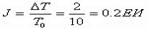 (assuming that the frequency of jitter less than 100 kHz). (assuming that the frequency of jitter less than 100 kHz).
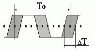
Fig. 2.1 Oscillogram of signal with jitter
At high levels of jitter, some systems may lose lock-on operation of frequency, and in the most severe cases - to loss of bit or frame synchronization. Typically, the presence of high jitter indicates bad quality equipment, strong interference, and malfunction in components.
For synchronization of networks most administrators of telecommunication networks are used by the method of hierarchical source - receiver (master - slave). The source of the main reference signal is one or more primary reference generator (PRG).The standard signal of this generator is distributed on a network which consist of generators - receivers or slave master clock (SMC).
The device used for the distribution of the reference clock signal can have a significant number of interruption events. The number of occurrences of the error packets can vary on average from 1 to 100 events per day, depending on the type of device, distance and other factors. For example, the requirement of characteristics significant damaged seconds for a through connection the (SDS) is equal to 175 events per day. SDS - a second of transmission, when occurs approximately 320 erroneous events CRS-6. This is equivalent to the bit error frequency 1x10⁻³ during a second. Requirements to characteristics in ANSI is 40-50 SDS per day, depending on the distance.
It should be said, that factors which result in skip, it is possible long to list, and if the transmission of clock signal is carried out through a radio contact, this list can have a great sizes because is added the row of problems which arise up at the transmission of signal through ether.
Summing up, it is possible to underline that we are not interested of origin nature of one or another hindrance or phase instability, interests us, that the system of selection of clock signal was as few as possible sensitive to them, and irresponsive on every indignation.
3 FUNCTIONING ANALYSIS OF PLL AS SLAVE SYNCHRONOUS GENERATOR IN DIGITAL COMMUNICATION CHANNEL
Phase-locked generator (Fig. 3.1) contains a phase comparator PD, inverter, generators of identical currents I1, I2, switches on the transistors VT1 and VT2, low-pass filter and synchronous generator VCO, voltage-controlled. The signal DIN comes from the communications channel at the entrance of the phase comparator
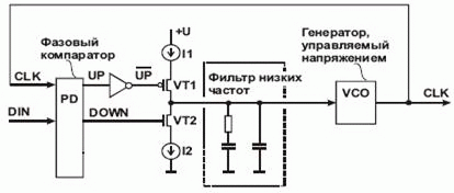
Fig. 3.1. Phase-locked loop
The phase comparator compares the signal DIN to clock CLK from the oscillator VCO. In order to achieve and then maintain the correct phase relationship between signals DIN and CLK, the phase comparator continuously monitors the phase error and generates control signals to speed up the UP and slow down DOWN pace of work the generator VCO.
The generator VCO with the nominal control voltage, approximately equal to U / 2, organizes a clock signal nominal (expected) frequency. Raising and reduction the voltage at the control input of the generator result in a slight increase and decrease the frequency. This allows to adjust the signal phase in the right direction.
The signals UP and DOWN (Fig. 3.1) control the transistor switches, regulating flow of currents I1 and I2 to the input of low pass filter. If UP = 0, DOWN = 0 transistors VT1 and VT2 are off, current sources are isolated from the filter and generator VCO, the voltage at the input of the generator remains constant or varies insignificantly because of the alignment of voltage on the filter capacitors, if initially these voltage do not coincide. When DOWN = 0 and goes series of pulses UP = 1, the transistor VT1 is switched on by each pulse, transistor VT2 is disabled, the current pulses I1 charges the capacitor, voltage at the input of generator VCO rises, the frequency of signal CLK slightly rises. If UP = 0 and goes series of pulses DOWN = 1 the situation is the opposite - the transistor VT2 is switched on by each pulse, transistor VT1 permanently closed, the current pulses I2 discharges the capacitor, the frequency of signal CLK is slightly reduced. When UP = 1, DOWN = 1, both transistors are switched on and as I1 ≈ I2, currents are practically compensated and the voltage at the generator VCO almost unchanged. In actual practice of the generator (Fig. 3.1) pulses UP and DOWN go take turns and often do not overlap. Thanks to low-pass filter, pulse effects on frequency of the generator VCO from the comparator is averaged.
As stated, the causes of sync species loss quite a lot. Quite often failures of synchronization in telecommunication systems is a result of jitter. It means that pulse is perceived by the phase comparator (PD) either before or after the required time. Therefore, the phase of the signal in the feedback loop is different from the phase of the signal comming from the communication channel and the system PLL begins the process of adjusting the phase. Naturally retiming takes time. Few or a lot of it depends on many factors, but during all this time, the communication system will stand, ie not be able to perform its functions. Therefore, if the noise immunity will be increase and makes the system less sensitive to noise and jitter, the failure and further recovery will occur much less frequently.
4 ANALYSIS OF EXISTENT PLL WITH INCREASED NOISE IMMUNITY
There are various ways of phase instability reducing. One such way is to use an adaptive filter to suppress the phase noise. The scheme of such a filter is shown in Fig. 4.1. It reduces distortion input signal which is introduced by the jitter and wander.
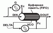
Fig. 4.1. Sheme of adaptive filter to suppress the phase noise
The scheme uses a buffer memory such as FIFO with indicator of level memory fill. This indicator generates a constant voltage DELTA, which is in sign and magnitude is proportional to the deviation of level memory filling from grades "50%".
Generator VCO, voltage-controlled, is capable under the influence of signal DELTA change the frequency within a small range. If DELTA = 0, the frequency output signal Fc is close to nominal. If DELTA > 0 frequency rises, if DELTA < 0 - goes down.
Assume that the buffer memory is filled to 50% in the initial state, the generator G with the phase locked loop picks out signal Ec, separator data (not illustrated) recovers data DIN and transmits them to the input of the memory. memory Data reading is controled by signal Fc.
In the presence of jitter in the signal Ec level memory fill performs relatively fast oscillations, which is reflected in the fluctuations of the voltage at the control input generator VCO. With enough inertia of the generator and the small slope of its voltage curve characteristic, signal Fc at the output is trembled to a lesser extent than the signal Ec, and the high frequency components of jitter are suppressed better than low frequency.
Just reduce the jitter can attenuator of fronts with jitter, whose structure is shown in Fig. 4.2. In standards for telecommunications equipment were introduced severe restrictions on the allowable jitter. Thus, according to the standard 62411 company AT & T, jitter should not exceed 2% of the period duration. To be specific, we take the standard T1 as example and will consider the work of attenuator. Transfer rate 1,544 Mbps, so a frequency of syncronization is 1,544 MHz. The duration of the signal period is approximately 648 ns, therefore, allowable jitter shall not exceed 12.96 ns.
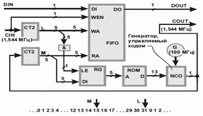
Fig. 4.2. Structure jitter attenuator and the sequence of states five-bit binary counters CT2. The numbers in the figure denotes the number of wires in the respective connecting lines
The attenuator includes a memory buffer such as FIFO, two five-bit binary counters CT2, five-bit logic element, five-bit register-latch RG, ROM, quartz generator G and a generator (NCO) which is managed by code. The inputs attenuator receives data signals DIN and synchronization CIN with unacceptably high levels of jitter. At the outputs of the attenuator formed corresponding signals DOUT and COUT with an acceptable level of jitter.
Attenuator operates as follows. The input data DIN is written to the buffer memory with an average speed of 1,544 Mbps. The instantaneous speed can differ from the average over the influence of jitter, so the level memory fill (the difference L - M) varies in time with fluctuations in the rate of input signals.
Periodically, after every 32 clock cycles the input signal CIN, triggered logic element AND, the difference of the counters stored in the register RG. If this difference deviates from the nominal (equal to 14 or 15), the constant which is read from ROM, acts on the generator NCO and slightly increasing or decreasing the frequency offset for indemnity of deviations.
Due to the inertia of the proposed system of automatic control, the output sync COUT reflects the average frequency of the input signal CIN and subjected to jitter only to the extent that is associated with the need to "thin" locked loop generator NCO. It means that the generator NCO will change the division factor. For example, if the frequency of generator is 100 MHz, the ratio will change from 64 to 65 and back. When the dividing coefficient hops from one value to another and back, fronts of output signal will be shake with an amplitude of 10 ns, but this is allowable jitter.
The above solutions can reduce the phase noise, but with a reduction in their frequency decreases the degree of attenuation. Also, the imperfection is a need for a substantial complication of the system. Using a large number of diverse elements, both analog and digital, complicates the process of concordance individual pieces of equipment and its tooling. This result in a large number of spoilage and complicates the production process of equipment. Therefore, creating a more simple way for interference suppression, using a small number of simple components would be fully justified. At the same time the sheme do not allow to struggle with the appearance of extra pulses, or conversely their disappearance, owing to appearance of any interference during transmission of clock signal, and a short duration of the reference signal loss will result in loss of synchronization.
5 DEVELOPMENT OF IMPROVED STRUCTURE OF SYNCHRONOUS GENERATOR WHICH IS BASED ON PLL
As already mentioned, the synchronization system may be influenced by various disturbances. In some cases ther are a broadening and narrowing of the pulse, or decay pulse and appearance surplus. But, as the noise are random, except for specially organized, often they manifest in one or two spurs, but not in the long flow. It means, that does not come some pulses of synchronization, but others will arrive in correct sequence. Or clock signal got some perturbations which the system can accept as the synchronization pulses, but then this sequence is correct. Instability phase also can manifest itself in one or two pulses, and then returned to the permissible limits. This condition can be used in the development of digital PLL for their improvement.
The shown below scheme makes the system PLL is insensitive to interference, which manifest themselves in several pulses, or in a small number of consecutive phase jumps (fig.5.1).
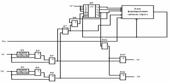
Fig. 5.1. Block of failure analysis
This scheme calculates the number of corrective impulses UP or DOWN. If their number is less than the specified number, the system considers them the result of the impact of noise and "does not pay attention to them". If is observed a large number of consecutive impulses, the scheme is turned off and allows to influence the VCO and rebuild frequency or adjust the phase.
This circuit was simulated in the package SystemView. Fig. 5.2 - 5.4 show the logic of the scheme when it is under the action of noise.
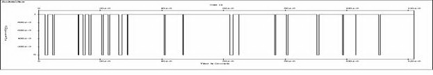
Fig. 5.2. Corrective impulses which are coming from the phase detector
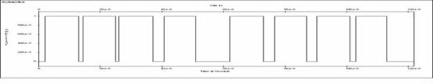
Fig. 5.3. The signal at the output of the counter
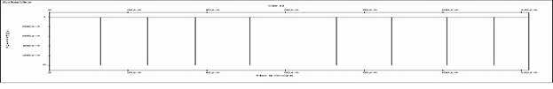
Fig. 5.4. Formed impulses of reset
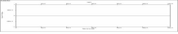
Fig. 5.5. Graph of transient in the system of PLL at influence of hindrances
When displacement of phase is or it is necessary to reconstruct frequency, there is occur blocking of analysis derangement block and all of system begins to work as ordinary PLL (fig. 5.6 - 5.8). This frequency tuning or phase is ended only five pulses later. Work of counters restored when the error signals from phase detector are stoped and thus is formed a reset signal.
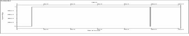
Fig. 5.6. The signal at the output of the counter
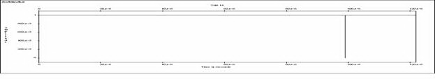
Fig. 5.7. Formed impulses of reset
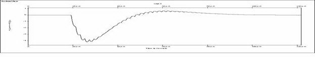
Fig. 5.8. Graph of transient in the system of PLL when is observed the displacement of signal phase
Simulation was also carried out for ordinary PLL. The results showed that with the same level of noise conventional system PLL loses capture mode and can not restore synchronism (Fig. 5.9).
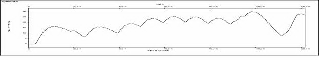
Fig. 5.9. Graph of transient in the ordinary system of PLL at influence of noise
The graph shows that with the advent of the first disturbance, the system starts the transient and tries to restore the tracking mode, but each successive interference again confuses the system, and it can not perform its functions. Block of failure analysis with the same level of interference is not responding to erroneous perturbations and continues to work in the steady state. This can be clearly seen in Fig. 5.5, which shows that during a noise, not some adjustment is not observed and the tracking mode is retained, and interference will not affect the system.
Thus, we do not lose much time when tuning frequency or phase is happened, but we get a good gain in noise immunity. The modeling showed that the scheme can work correctly with the noise level above 20% - 30%, than for conventional digital PLL system.
CONCLUSIONS
In this paper we consider a system synchronization. It is shown that its quality is directly related to the quality of services provided. The reasons for reduced quality of sync quite a lot and at each specific performance of synchronization network is had its own set. In most cases, to highlight the clock transmitted over the communications channel, using the scheme, made on the basis of phase-locked loop (PLL). And if there was a failure of synchronization, the functions to restore is assigned on the system PLL, which adjusts the frequency or adjusts the phase. Digital PLL system has a rather bad noise immunity and therefore any impact of noise or phase instability lead to loss of synchronism.
The paper discusses some options for reducing phase noise, but they require a significant complication of the device and can not struggle with slip. Therefore proposed a simple scheme to struggle with slip and phase instability. This scheme has been simulated in SystemView. The modeling showed that noise immunity system rises by 20% - 30%. The system does not respond to incoming short-lived perturbation and slip. The scheme also allows the regime to maintain synchronism with the outage of the reference signal coming from the communication channel. And if the signal will not be absent for a long time, this failure will not influence system work.
Literature
- Ковязин Д.А. Отчет по производственной практике на ОАО «ЕГУЭС Уралтелеком» [electronic resource] / Д.А. Ковязин / - Access mode to article:
http://www.bibliofond.ru/view.aspx?id=105073
- Карпенко Л.В. Передача сигналов синхронизации аппаратурой PDH [electronic resource] / Л.В. Карпенко / - Access mode to article:
http://www.nateks-dv.ru/Publications.aspx?publicationID=63
- Сухман С.М. Синхронизация в телекоммуникационных сетях. Анализ инженерных решений / С.М. Сухман, А.В. Бернов, Б.В. Шевкопляс – М.: Эко-Трендз, 2005 – 260 с.
- Слепов Н.Н. Синхронные цифровые сети SDH. – 4-е исправ. изд. / Н.Н. Слепов – М.: Эко-Трендз, 1999. – 150 с.
- Слепов Н.Н. Синхронизация цифровых сетей. Методы, терминология, аппаратура [electronic resource] / Н.Н. Слепов / - Access mode to article:
http://www.electronics.ru/issue/2002/2/4
- Щеланов Л.Н. Основы теории тактовой сетевой синхронизации [electronic resource] / Л.Н. Щелованов, Г.С. Антонова, Е.М. Доронин, С.В. Рыжкова / Access mode to resource:
http://www.dvo.sut.ru/libr/opds/i052shel/index.htm
- Давыдкин П.Н. Тактовая сетевая синхронизация / П.Н. Давыдкин, М.Н. Колтунов, А.В. Рыжков. – М.: Эко-Трендз, 2004 – 205 с.
- Стариков О. Метод ФАПЧ и принципы синтезирования высокочастотных сигналов [electronic resource] / О. Стариков / Access mode to article:
http://chipnews.gaw.ru/html.cgi/arhiv/01_06/stat-6.htm
- Клэппер Д. Системы фазовой и частотной автоподстройки частоты / Д. Клэппер, Д. Фрэнкл / пер. с англ. под ред. А.Ф. Фомина – М.: Энергия, 1977 – 440 с.
- Максимов М. В. Защита от радиопомех / М. В. Максимов, М. П. Бобнев, Б. X. Кривицкий, Г. И. Горгонов, Б. М. Степанов, Л. Н. Шустов, В. А. Ильин. – М.: Советское радио, 1976 – 485 с.
аutobiography | DonNTU | masters portal
RUS | UKR
|

