


1. Introduction
2. General concepts
3. Classification of RAM
3.1 Static random access memory
3.2 Dynamic random access memory
4. Organization of main memory
4.1 The organization of MM that based on the block scheme
4.2 The organization of the MM on the basis of the block interleaving scheme with a cyclic pattern
4.3 Organization of the MM on the basis of a block design with block-cyclic scheme bundles
Conclusion
Bibliography
Important Note
1. Introduction
Computing the direction of the use of computers has always been the main engine of progress in
computer technology. As the main characteristics of computers used indicators such as the performance —
the value that shows how the number of arithmetic operations it can perform per unit time. That performance
is most clearly demonstrates the extent of progress made in computer technology.
In any CMs, regardless of its architecture, programs and data stored in memory.
Memory functions are provided by storage devices (memory), intended for fixation, storage
and delivery of information in the course of the CM.
Theme analysis of the functioning
of main memory with block-cyclic pattern of the bundle is relevant in our time, because the building block
of memory has important advantages such as reducing the time information access and compliance to building capacity.
This is possible due to the potential parallelism inherent to the block of the organization. Greater access speed can
be achieved by simultaneous access to many memory banks.
The aim was to analyze the functioning of the main memory with
block-cyclic pattern of the bundle.
We can distinguish the following tasks master's thesis:
- Review of methods of analysis of the functioning of main memory
- Construction and implementation of Markov models of main memory with block-cyclic scheme bundles
- Analysis of main memory, based on block scheme
- Analysis of main memory interleaving in a cyclic scheme
- Analysis of main memory with block-cyclic scheme bundles
Expected practical results are to make recommendations on the organization of the volume of banks and
blocks according to type of criteria for reliability or speed.
Scientific innovation is the development and
implementation of Markov models of main memory with block-cyclic scheme of the bundle.
2. General concepts
Main memory (MM) — the only type of memory that can go directly
to the CPU (except the registers of the CPU). Once the information stored on external memory to be rewritten to main
memory, it becomes accessible to the processor.
MM consists of storage devices with random access. Such storage
devices are organized as an array of cells. Each cell has a unique address and contains a fixed number of storage elements.
Unique address allows us to distinguish cells that are accessed to perform read and write.
Appeal to any cell is one
and the same time and can be performed in a random sequence (random access).
3. Classification of RAM
Main memory can include two types of devices:
• read-only memory (ROM)
• random access memory (RAM)
1) Read-Only Memory (ROM)
Smaller proportion of main memory ROM image (ROM — Read-Only Memory). Unlike RAM, they provide a readout
of information, but do not admit of change (there are some cases when the information in ROM can be changed,
but the process is different from reading and requires much more time).
ROM chips volatile.
2) Random Access Memory (RAM)
Larger share of the basic form of RAM memory (RAM — Random Access Memory),
called operational, because they permit the same type, produced virtually the same speed,
the operation of recording and reading information (via electrical signals).
But keep in mind that the RAM chip can be used only as a temporary memory,
because it must be permanently connected to a power source.
There are two
basic types of memory-access:
• static (SRAM — Static RAM)
• dynamic
(DRAM — Dynamic RAM)
Let us examine them in detail.
3.1 Static random access memory
Static RAM — it's the fastest, though, and the most expensive type of RAM. Allocated a number of different variants of SRAM, different technology, methods of organization and scope (Fig. 1).
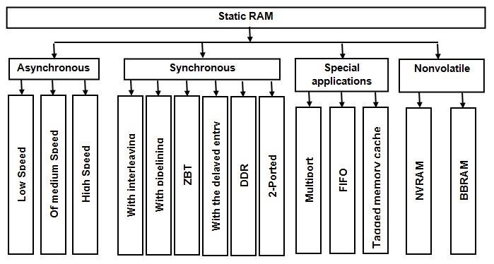
Figure 1 — Types of Static RAM
Asynchronous static RAM.
Asynchronous static RAM used to cache the second
level for many years (since the advent of the microprocessor i80386). For these ICs access
time is 12-20 ns, which is not allowed to cache the second level to work in temperatures of
the processor.
Synchronous static RAM.
Within this group of static RAM
ICs secrete type SSRAM and PB SRAM (better).
Compared with asynchronous static RAM, a much
better performance achieved in the synchronous SRAM (SSRAM). All events in SSRAM occur with the
arrival of external reference clock. A distinctive feature of SSRAM are input registers, where it is
fixed input.
Last modification microprocessors Pentium, starting with Pentium II, equipped with a
static random access memory with pipelined packet access (PB SRAM — Pipelined Burst SRAM), instead SSRAM.
Due to internal pipelining in PB SRAM, the rate of exchange of data packets increases by about half. The
memory of this type works well at higher frequencies the system bus. The access time for PB SRAM ranges from
4.5 to 8 ns.
3.2 Dynamic random access memory
It is used in DRAM main
memory CM, therefore, a dynamic memory in a computer much more than static.
As well as SRAM, dynamic memory
consists of a nucleus (solid EM) and an interface logic (buffer registers, amplifiers read data recovery circuits,
etc.). Number of DRAM has already exceeded two dozen, but the kernel they have organized almost identically, the
main differences are related to the interface logic (well, they are due, and the scope of chips). Classification
of dynamic memory chip shown in Fig. 2.
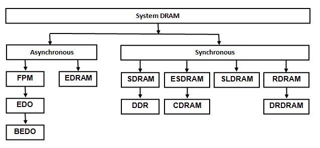
Figure 2 — Classification of dynamic RAM. Chips for main memory
4. Organization of main memory
To implement the main memory
is used to combine several integrated circuits (ICs). The reason for the association is large capacity RAM and
excess bit words BM discharge cells chip memory.
The increase in the bit memory is realized by combining
address inputs merged memory ICs. Information inputs and outputs of ICs are the inputs and outputs of the module
memory increasing discharge (Fig. 3).
The collection of chips is called the memory module. One or more
modules to form a memory bank.

Figure 3 — The increase in the bit memory (Animation: volume — 40.8 Kbytes, the number of frames — 6, size — 559 x 280)
To obtain the required storage capacity must be some
way to combine several smaller capacity memory banks. In general, the main memory of VM is almost always
has a block structure (contains some banks).
When using a block of memory, which consists of Banks,
the cell address A is converted into a pair (b, w), where b — number of the bank, w — cell address inside
the bank.
Distribution schemes of discharges address and between b and w:
• block (the number of
bank b determines the most significant bits of address);
• cyclic (b = A mod B; w = A div B);
• block-cyclic (a combination of the two previous schemes).
4.1 The organization of MM that based on the block scheme
Consideration of the basic structures of the MM block for the example of the memory capacity of 512 words constructed from the four banks of 128 words each. The structure of memory, organized in accordance with this structure, shown in Fig. 4.
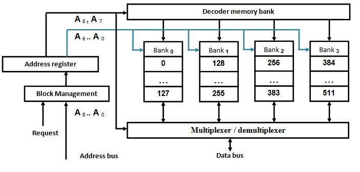
Figure 4 — Outline of main memory, based on block diagrams
Memory address space
is divided into groups of addresses (consecutive), each group is provided by a separate memory banks.
To access the OP uses 9-bit address. Seven LSBs (A6-A0) are fed in parallel to all memory banks
and choose in each single cell. Two senior level address (A8, A7) contain a number of the bank.
Choosing a bank is provided either by multiplexing information, or using a decoder bank number.
In functional terms, this MM can be regarded as a memory, whose capacity is equal to the total
capacity of components, and speed — speed of an individual bank [1].
4.2 The organization of the MM on the basis of the block interleaving scheme with a cyclic pattern
The advantages of a block of memory may include building
capacity and reducing the time to access information due to potential overlap.
Access speed
increases due to the simultaneous access to many memory banks. One of the techniques used for this
purpose is called a bundle of memories. It is based on the so-called interleaving (address interleaving),
is a change in the distribution system addresses between the memory banks.
Interleaving is provided by the cyclic decomposition address. In this case
(Fig. 5) to select the bank, two junior level addresses (A1, A0), and to select
the cell in the bank — 7 significant bits (A8-A2).
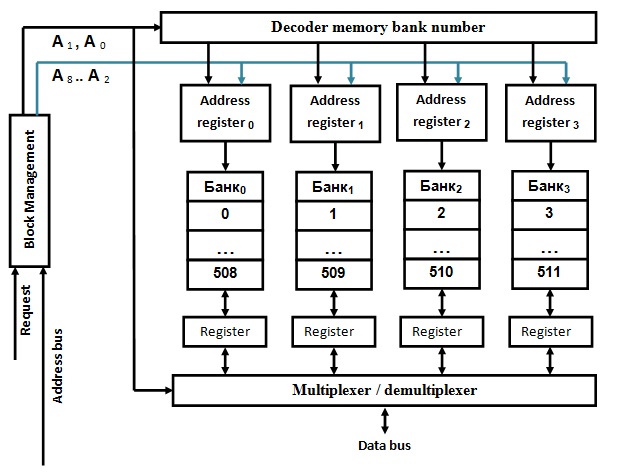
Figure 5 — Block interleaved memory with a cyclic pattern
Sequential access memory is usually performed on cells that have adjacent addresses.
Can be achieved in B (B — number of banks) times the speed, exchange, memory as a whole
than its individual bank, if the simultaneous sequential data access in each of the banks.
If the requests to the same bank to follow one another, each subsequent request must
wait for completion of previous service. This situation is called a conflict of access.
With frequent occurrence of conflicts on access method becomes inefficient
4.3 Organization of the MM on the basis of a block design with block-cyclic scheme bundles
In a block-cyclic scheme bundles, each memory bank consists of several modules, addressable in a circular pattern. Addresses are distributed among the banks on the block diagram. Address of the cell is divided into three parts. High-order bits define the number of the bank, the next group of digits indicates the address of a cell in the module, and the younger address bits select a module in the bank (Fig. 6).
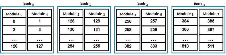
Figure 6 — A block-cyclic scheme of separation of memory
Conclusion
The above methods of separation of memory work
well in solving a problem, characterized by a locality property. In multiprocessor systems with
shared memory, where requests for access to memory is independent, is considered the development
of the idea of separation of memory. To this end, the system includes multiple memory
controllers, allowing individual banks to work completely independently.
The effectiveness of this technique depends on the frequency of independent
accesses to different banks.
The greater the number of banks, the less
likely the successive calls to the same memory bank.
Bibliography
- Цилькер Б.Я. Организация ЭВМ и систем [Текст]: — М : ПИТЕР, 2004. — 668 с.
- Столингс У. Структурная организация и архитектура компьютерных систем [Текст]: — М. : Вильямс, 2002. — 893 с.
- Оперативная память [Электронный ресурс]. — Режим доступа: http://ru.wikipedia.org/wiki/Оперативная память
- Шпаковский Г.И. Организация параллельных ЭВМ и суперскалярных процессоров [Текст]: — Мн.: Белгосуниверситет, 1996. — 296 с.: ил.
- Халабия Р.Ф. Организация вычислительных систем и сетей [Текст]: — М. : МГАПИ-Москва, 2000. — 141 с.
- Фельдман Л.П., Михайлова Т.В. Вероятностная модель блочной памяти // Искусственный интеллект.— Донецк: ІПШІ МОН і НАН України “Наука і освіта”, 2010.
- Мюллер C. Модернизация и ремонт ПК, 18-е издание [Текст]: пер. с англ. — : ООО «И.Д. Вильямс», 2009. — 1280 с.
- Алиев Т.И. Основы моделирования дискретных систем [Текст]: — СПб. : СПбГУ ИТМО, 2009. — 363 с.
- Букатов А. А., Дацюк В. Н., Жегуло А. И. Программирование многопроцессорных вычислительных систем [Текст]: — Ростов-на-Дону : ООО «ЦВВР», 2003. — 208 с.
- Архитектура компьютера [Электронный ресурс]. — Режим доступа: http://itblock.ru/
Important Note
At the time of writing this abstract master thesis is still not complete. Expected completion date: December 1, 2011, as a consequence of the full text, as well as materials on the subject can be obtained from the author or his manager after that date.