Broad Band Software-Defined Radio Receivers Based on Superconductive Devices
Авторы: Akira Fujimaki, Koichi Nakazono, Hiroaki Hasegawa, Takashi Sato, Akira Akahori, Nobuo Takeuchi, Futoshi Furuta, Masaaki Katayama, and Hisao Hayakawa
Источник: IEEE Transactions on Applied Superconductivity, Vol II, No I — 2001
Abstract
We have studied software-defined radios (SDRs) based on superconducting devices. The increasing data rate in mobile communications will require a band-width of up to a few hundred MHz in the future. We have confirmed numerically the broad-band characteristic of oversampled analog-to-digital converters including a lowpass and bandpass modulator. Furthermore, the bandpass modulator constructed without a resistor is found to have sensitivity improved by two orders of magnitude compared to that of the lowpass modulator. This result means that the digital RF radio architecture based on a bandpass ADC is better suited for a future SDR receiver.
I. Introduction
As is well known, there is rapidly increasing traffic in mobile wireless communication networks. The annual rate of increase in handsets including PHS (Personal Handy Phone System) has reached 140% over the past 5 years in Japan. This growth will continue until the multimedia communication systems are well established.
Reflecting such a growth, the mobile communication system has already used a variety of air interfaces and bands. For example, digital cellular phones with time domain multiple access (TDMA) technology have the allocated frequencies around 850 MHz, while analog cellular phones are active in the same frequency band. In addition, a new service CDMAOne based on the code division multiple access (CDMA) has already started around 850 MHz. In 2001, the advanced service cdma2000 or W-CDMA will come to the market. New radio standards and advanced services are proposed, one after another, to be added to the legacy services. This rapid change shortens the lifetime of a given standard or service, and, shortens the lifetime of handsets and basestations. In particular, the short lifetime of the base-stations causes severe problems, because all the base-stations existing over the whole area should be upgraded to the new service at the same time. This entails much time and cost. Thus, future base-stations will be required to have high flexibility and reconfigurablity. However, present technology, based on analog components, offers limited flexibility and reconfigurability.
Although the concept of the software-defined radio (SDR) was conceived for military applications, the SDR technique may have commercial applications, because the radio has the ability to satisfy the flexibility requirement. In the SDR, the functions are redefined in software, e.g., by softwaredownloads or subscriber identity cards.
Recently, our group has proposed an advanced base-station [
In this paper, we describe the direction of the research on the superconducting SDR receivers. We also report our challenge to the development of superconducting devices for the SDR receivers.
II. Requirement for Future SDR Base Stations
A. Bund Width
According to the white paper from the Ministry of Postal Service and Telecommunication of Japan [5], the data rate for a single subscriber will continue to increase as well as the number of subscribers for the near future. The required data rate for mobile communications will reach a few tens of Mbps in 2010, though the present data rate is no more than 64kbps.
A single base-station should cover several subscribers inside a cell. Thus, the future base station has to have capability to handle a band width as high as 100MHz or more. Network providers point out that larger cell sizes leading to broader band widths are preferable because the maintenance cost of the base-stations can be suppressed, though the larger cell size is less efficient use for frequencies.
Figure 1 shows the schematic view of the multimode radio based on a conventional multi-hardware receiver and SDR in terms of channel selection. The conventional receiver is composed of frequency-fixed analog components including mixers and bandpass filters as shown in Fig. 2(a). Channel selection is performed through the bandpass filter placed at the RF stage.
On the other hand, a large block of the cellular spectrum containing multiple channels is selected in the analog bandpass filter at SDR receivers. The broad-band signals are digitized using a single broad-band analog-to-digital converter (ADC), then the desired individual channel is extracted from the digitized signals through the software-defined channel selection filter as shown in Fig. l(b) [6]. This architecture yields high flexibility. Future SDR receivers should have capability to cover multiple channels each of which have the band width of about 100MHz, so that the band width of the SDR receiver is required to be much greater than 100MHz. The ADC used in the SDR receiver needs to have such a broad band width.
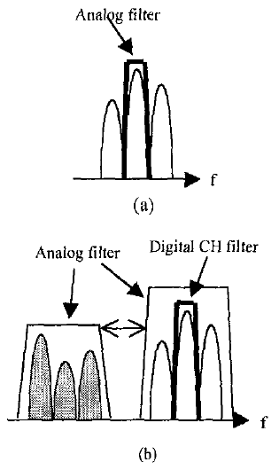
Fig. 1. Channel selection for a conventional narrow-band receiver (a) and an SDR receiver (b). An analog filter selects a whole system to be covered with the receiver in SDR, while only one channel to be used is selected in a conventional receiver. Channel selection is performed in a digital domain for SDR. If largely tunable filters can be employed, the detectable spectrum is enhanced largely and flexibility in the system selection is enhanced for SDR.
If the center frequency of the RF filter is varied largely (see Fig. 1(b)), the covered spectrum is enhanced effectively. As a result, flexibility is enhanced in some cases, even if a lower band-width ADC is adopted.
B. Architecture
We have already described elsewhere the different SDR architectures with which the receiver chain from RF to base-band is formed [2]. The first architecture shown in Fig. 2 (b) is referred to as "the digital baseband radio". The second one indicated in Fig. 2 (c) is also referred to as "the digital EW radio". When the base stations are constructed, digital filters are required for each channel. These architectures have high flexibility to enable changes in the systems’ features such as the modulation scheme, allocated frequency band. Broad- band superconducting RF filters and broad-band ADCs are essential for each architecture as discussed below.
The common benefits of using superconducting devices in these architectures come from the employment of the superconductor ADC. As mentioned above, an input band-width of greater than 100MHz is needed for a future SDR receiver. However, the band-widths of conventional, non-oversampled semiconductor ADCs are limited by clock jitter [7]. Due to this limiting factor, the enhancement rate of the band-width for semiconductor ADCs is suppressed to be 115%/year. Using this rate, the input band-width can be estimated to be 200MHz for 12-bit ADCs and 50MHz for 14-bit ADCs by 2010. When we employ the oversampled ADCs [8–11], the effect of the clock jitter can be reduced considerably [12]. The superconductor oversampled ADCs based on single-flux-quantum (SFQ) logic can operate at frequencies of several tens of GHz, which is 1- or 2-orders of magnitude higher than the clock frequency of a semiconductor oversampled ADC. This high clock frequency of superconductor ADCs enables us to break the barrier of the clock jitter limit and to enhance the input band-width.
Another advantage of SFQ-based ADCs is high sensitivity. The minimum power of input signals required to drive SFQ circuits is less than 1μW, while that of high-speed semiconductor ADCs is around 1mW. The nature of high sensitivity brings the reduction in the gain of the LNA by 30dB. Usually, the product of the gain and bandwidth is considered constant for a given amplifier. Thus, the reduction in the gain enhances the band-width covered by the LNA, widening the frequency band. As described later, a bandpass modulator of superconductor Σ–Δ ADC yields extremely high sensitivity. In that case, the LNA can be removed from the receiver chain as shown in Fig. 2(c), and the noise figure will be improved by a few dB. Taking into account that RF signals are difficult to digitize directly in semiconductor ADCs, superconductor SDR receivers have a great advantage in the digital RF radio in which the bit error rate of the receiver will be improved remarkably [2].
In addition to the SFQ-based ADCs, analog bandpass filters made of superconducting films are required. The low loss nature enables us to make the multi-stage thin-film filters with lower insertion loss and broad band-width.
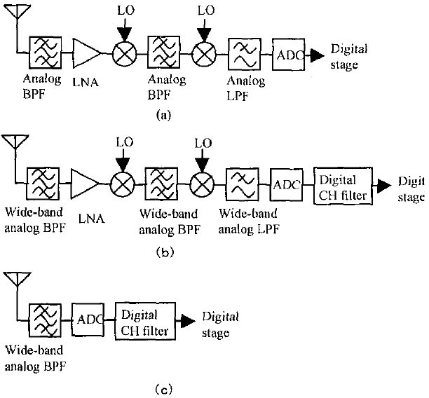
Fig. 2. Configuration of a receiver chain for a single channel. (a) Conventional narrow-band heterodyne receiver. (b) Digital-baseband radio.
III. Development of Superconducting Element
In this section, we focus on our study of superconducting ADCs. Figure 3 shows the equivalent circuit of a 1st-order lowpass Σ–Δ modulator designed in this work. Such a modulator can be employed in the digital base-band radio indicated in Fig. 2 (b). The junction J2 acts as a comparator. The integrator is composed of the resistor R1 and inductor L1, and cut-off frequency is designed to be 12.5MHz. To improve signal-to-noise ratio (SNR) [13], we amplify the output signal and feed it back to the integrator. The amplifier is formed by the ladder circuits which are composed of Josephson Transmission Lines (JTLs), splitters, and confluence buffers. Five SFQ pulses are produced for one input SFQ in the ladder circuit. The five pulses come back to the integrator through the junction J4 and one pulse is fed back inherently through the comparator J2. As a result, six SFQ pulses accompanying opposite circulating currents are fed back, resulting in the reduction of the current flowing at J2.
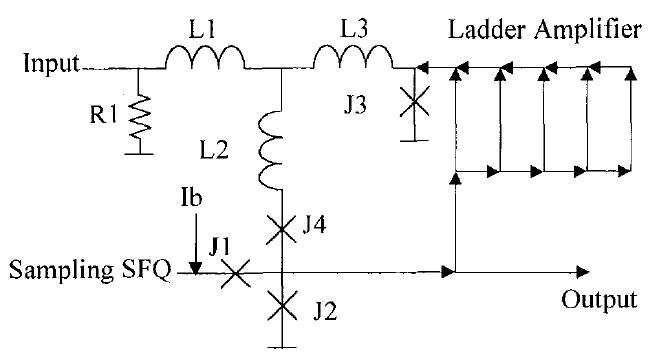
Fig. 3. Equivalent circuit ofthe lowpass modulalor for the Σ–Δ ADC. The amplifier with a ladder structure enhances SNR. The circuit parameters are as follows: J1=J4=100μA, J2=J3=140μA, R1=2.5mΩ, L1=200pH, L2=2pH, L3=8pH.
Figure 4 shows the numerically obtained noise power density as a function of frequency for the circuit shown in Fig. 3. We display both results with and without using the amplifier, to examine the effect of the amplifier on SNR. The output waveform with the clock frequency of 20GHz is calculated by using JSIM [14], then forwarded to a Fast Fourier Transform function. The calculated noise density is normalized by the full-scale signal applied at 220MHz. It is evident from the figure that the noise shaping is accomplished as expected. In addition, SNR of the modulator with the amplifier is enlarged by about 5dB compared to that without amplifier at low frequencies. However, there are the same levels of spurious between the two. Moreover, the calculated SNR is still insufficient for the receiver application. We have to design second or higher order modulator.
Figure 5 shows a photomicrograph of the modulator with a ring oscillator working as a clock generator. The chip is fabricated using the NEC standard process based on Nb/AlOx/Nb junction technology with Jc of 2.5kA/cm2 [15]. The modulator operates correctly at low frequencies. High frequency testing is in progress.
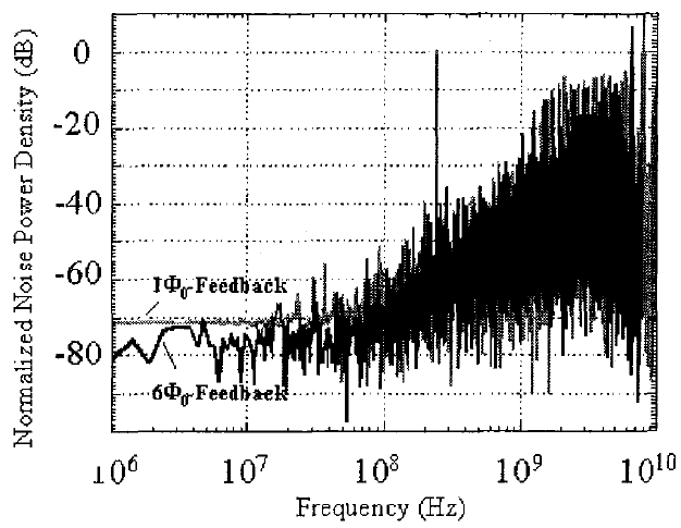
Fig. 4 Power spectrum of quantization noise normalized by a full- scale signal. "1Φ0-fecdback" and "6Φ0-feedback" correspond to the result without and with the amplifier, respectively.
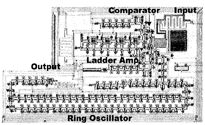
Fig. 5. Photomicrograph of a fabricated lowpass modulator
In second or higher order lowpass modulators consisting of a resistor, inductor and junction, the full-scale signals reach at least a few mA in amplitude. This relatively high amplitude, which is dominantly due to the use of the resistor, requires an appropriate amplifier before the lowpass modulator.
On the other hand, a bandpass Σ–Δ modulator consisting of a capacitor, inductor and JJ shows high sensitivity. Figure 6 shows the equivalent circuit of the bandpass modulator proposed first by the group of Northrop Grumann [16]. This modulator has the tank circuit composed of the inductor L and capacitor C. The resonant frequency is designed to be 2GHz. The tank circuit serves as a resonator yielding the quantization noise shaping for bandpass use, though the circuit acts as the second-order lowpass filter for analog input signals.
The calculated noise spectrum is shown in Fig. 7. The clock frequency is set to be 20GHz and the junction parameters are made to meet the NEC standard process. The noise is normalized by the full-scale signal applied at 1.95GHz. Evidently from Fig. 7, the bandpass characteristic of the noise shaping can be obtained around the resonant frequency. The spurious-free dynamic range is calculated to be 62dB for the band-width of 100MHz at the center frequency of 2GHz.
The amplitude of the full-scale signal is no more than 22μA, which is 2 orders of magnitude smaller than required for the lowpass modulator. This extremely high sensitivity enables us to remove any amplifier from the receiver chain in the digital- RF radio as indicated in Fig. 2(c). The noise figure will be improved by a few dB, which is vital for radios having higher carrier frequencies.
As mentioned before, largely tunable analog filters help yield flexibility in SDR receivers, We have started to develop the tunable filter in cooperation with Kinki University. The filter consists of a superconducting thin film filter and a plate of a magnetic or dielectric material. The plate is set above the filter, and the center frequency is controlled by changing the distance between the filter and the plate. We have obtained a change in the center frequency of about 640MHz for the initial center frequency of 3.5GHz with preliminary measurements. Here, we use LSAT as the dielectric material. A larger change could be obtained by optimizing the structure. The details including insertion loss and distortion will be discussed elsewhere [17].
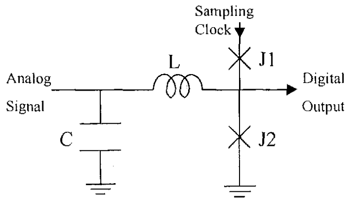
Fig. 6. Equivalent circuit of a bandpass modulator for a Σ–Δ ADC first proposed by Ref.15. The resonator is composed of L of 100pH and C of 63pF.
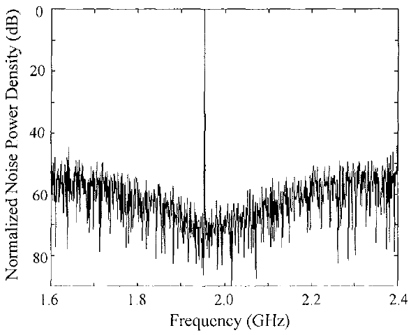
Fig. 7. Power spectrum of quantization noise normalized by a full-scale signal for the bandpass modulator of Σ–Δ ADC.
IV. Summary
We have studied superconductor-based software-defined radios applicable to future base-stations. Considering the trend in the data rate of mobile communications, a future receiver will have to cover a band-width greater than 100MHz. Thus, an SDR receiver should be composed of a broad-band analog filter and a broad-band ADC, in which the superconducting devices have advantages over semiconductor devices. In particular, the numerical analysis shows that the digital RF radio architecture based on the bandpass ADC without a resistor has high performance in sensitivity. The lowpass ADC has high potential for broad-band, relatively low sensitivity applications as well as the bandpass ADC.
Acknowledgment
A. F. thanks Prof. Hontsu of Kinki Univ. for his fruitful discussion on tunable filters.
References
1. A. Fujimaki, and M. Katayama, "Toward the Intelligent Super Basc- Station with software defined radio techniques and superconductive devices," Technical report of IEICE, CAS-98. pp. 85-92, March 1999. (in Japanese)
2. A. Fijimaki, M. Katayama, H. I-layakawa, and A. Ogawa, "Advanced base-station based on superconductive devices and software-defined radio technology," Supercond. Sci. & Technol., Vo1.12, No. II , pp.708–710, Nov. 1999.
3. A. Pujimaki, "Application of superconducting tcchnology to future wireless communication systems," Extend. Abst. of the 4th Joint ISTEC/MRS Workshop on Supercond., pp, 186-189, Kauai, HA., 1999.
4. E. B. Wikborg, V. K. Scmenov, and K. K. Likharev, "RSFQ front-end for a software radio receiver," IEEE Trans. Appl. Supercond., Vol. 9, No. 2, pp.3615-3618, June 1999.
5. 1997 Policy Report of Telecommunication, Printing Bureau, Ministry of Finance of Japan, 1997. (in Japanese)
6. H. Tsurumi and Y. Suzuki, "Broadband RF stage architecture for software-dcfined radio in handheld terminal applications," /EEL Commim. Mag., pp.90-95, Feb. 1999.
7. R. H, Walden, "Performance trends for analog-to-digital converters," lEEECommtm. Mag., pp.96-101, Feb. 1999.
8. V. K. Semenov, Y. A. Polyakov, and T. A. Filippov, "Analog-to-digital converters with on-chip digital low-pass filters," IEEE Trans. Appl. Supercond., Vol. 9, No. 2, pp.3026-3029, June 1999.
9. S. V. Rylov, D. K. Brock, D. V. Gaidarenko, A. F. Kirichenko, J. M. Vogt, and V. K. Semenov, "High resolution ADC using phase modulation-demodulation architecture," IEEE Trans. Appl. Supercond., Vol. 9, No. 2, pp.3016-3019, June 1999.
10. A. H. Worsham, D. L. Miller, P. D. Dresselhaus, and J . X. Przybysz, "Superconducting modulators for high dynamic range delta-sigma analog-to-digital converters," IEEE Trans. Appl. Supercond., Vol. 9, No. 2, pp.3157-3160, June 1999.
11. D. L. Miller, J. X. Przyhysz, and A. H. Worsham, "Flux quantum sigma-delta analog-to-digital converters for rf signals," IEEE Trans. Appl. Suprcond., Vol. 9, No. 2, pp.4026-4029, June 1999.
12. S. R. Norsworthy, R. Schreier, and G. C. Temes, Delta-sigma data converters, IEEE Press, 1997, chap. II
13. J. X. Przyhysz, D. 1 ,. Miller, and E. N. Naviasky, "TWO-loop modulator for sigma-delta analog to digital converter," IEEE Trans. Appl. Supercond., Vol. 5 , No. 2, pp.2248-2251 , June 1999.
14. E. S. Fang and T, V. Duzer, "A Josephson integrated circuit simulator (JSIM) for superconductive electronics application", Extend, Abst. of 1989 Int. Superconductive Electronics Conf, pp, 407-410 , Tokyo 1989.
15. S. Nagasawa, Y. Hashimoto, H. Numata and S. Tahara, "A 380ps, 9.5mW Josephson 4-Kbil RAM operated at a high bit yield", IEEE Trans. Appl, Supercond., vol. 5, pp. 2447-2452, Jun. 1995.
16. J. X. Przyhysz, U.S. Patent 5341136.