 |
| Faculty: Computer Science |
| Speciality: System programming |
| Theme of master's work: Research methods for processing color images |
| Scientific adviser: Samoshchenko Alexandr |
Abstract:
"Research methods for processing color images"
Introduction, relevance, purpose and objectives
What is image? This question can be answered in different ways. The most simple and broad definition of this concept is that image is what we see. Another definition: an image is information that is suitable for visual perception. Depending on the origin there can be described types of images:
- Draw or print (artist, printing, printer).
- Optical (intensity distribution of the electromagnetic field generated by an optical device in a certain region of space, for example, on the retina, at the screen projecting, in the plane of the receiver of the camera lens).
- Photographic (optical image recorded on the photos from a chemical process).
- Electronic or Digital (optical image recorded by an electronic receiver, such as CCD, scanner).
Currently, there are many storage formats and compression algorithms graphics: raster formats (BMP, ECW, GIF, ICO, ILBM, JPEG, JPEG 2000, MrSID, PCX, PNG, PSD, TGA, TIFF, HD, Photo), vector format (Scalable Vector Graphics (SVG and SVGZ), Encapsulated PostScript (EPS)), Metafiles Windows: WMF, EMF, files CorelDraw: → CDR, CMX, Adobe Illustrator (AI), XAR.
At this stage the algorithm analyzes of the image compression JPEG is making. The algorithm has a fairly complicated math, in which the operations of multiplication, division and addition of matrices are present. This is a fairly laborious process that requires some hardware resources for its implementation, but not always solve the problem of speed. The direction of improved performance is the hardware implementation of some parts of the algorithm, which requires the use of sophisticated instruments and large hardware resources. In this case, the most effective option is to use a hardware implementation of programmable logic integrated circuits (FPGAs).
FPGAs have recently become more common element base for use in devices for digital signal processing (DSP). With advanced architecture, high clock frequency and low cost FPGAs are indispensable for prototyping and small batch production.
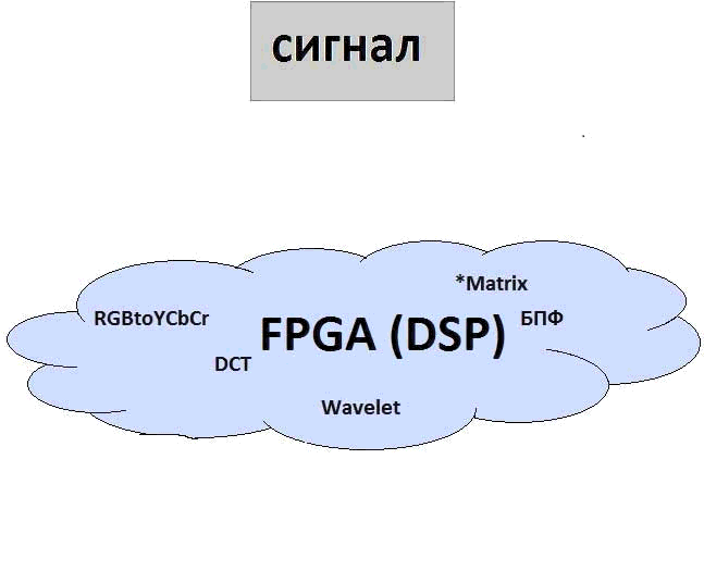
Figure 0 — Example using FPGA
Animation. The number of frames — 4. Size — 115 Kb. The number of repetitions — 5
At the current stage the task is to study methods of converting a color image from one model to another and implement it on the FPGA to improve the performance of the algorithm. At the moment we consider a model image conversion from RGB format to the chroma format is YCbCr. This is the first step in the algorithm of compression JPEG.
The scientific importance and the main results
The resources of FPGA to perform the multiplication and multiply‐accumulateAs is known, the performance of hardware implementation of algorithms is much higher than software. The circuit architecture of FPGA, the full name of which sounds like a Field Programmable Gate Array (programmable basic matrix chip), is currently concentrated in itself the latest technological advances in microelectronics and gives developers the most advanced capabilities. The development of FPGA architecture associated with the permanent addition of equipment to facilitate the execution of operations of digital signal processing. This primarily concerns multiply. The main resource of the programmable chip architecture FPGA — the so‐called logic cell. It is composed of the generator logic functions, whose work is given a truth table (Look‐Up Table ‐ LUT), a trigger and a number of specialized resources, simplifying the implementation of typical digital circuitry nodes. [1]
The structure of each logic cell includes the following accessories:
- The chains of accelerated transfer intended for the rapid transmission of cary‐bits between logic cells, which simplifies the organization of multibit nodes.
- Block memory.
- Dedicated Multipliers: specialized units that perform the multiplication of independent 18‐bit operands at frequencies up to hundreds of megahertz (for families of Spartan‐3E — 266 MHz). At a certain stage of development of PLD revealed that programmable logic can be regarded as an effective co‐processor digital signal processing (DSP). The possibility of implementing parallel algorithms on‐chip FPGA significantly improves their position in relation to common signal processors. These conditions are realized mainly in cases where the solution requires a large number of multiply‐accumulation, especially in algorithms transform the different formats for images.[2]
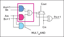
Figure 1 — Valve MULT_AND, designed to accelerate the multiplication operations in the logic cells
When implementing algorithms using multiply‐accumulates for a stream of input data, often one and the same data stream is necessary to multiply at the same time on different factors to the accumulation of the sum separately for each of the channels multiply. To implement these algorithms for multiplication blocks on a chip have an additional input that can connect to the cascade output of the preceding multiplier in the column (Fig. 2).[2]
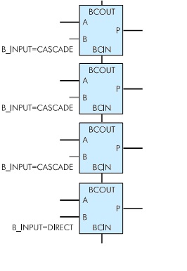
Figure 2 — cascading multiplier
The Xilinx RGB to YCrCb Color‐Space Converter LogiCORE™ is a simplified 3x3 matrix multiplier that converts three input color samples to three output samples in a single clock cycle. The optimized structure uses only four XtremeDSP™ slices by taking advantage of the dependencies between coefficients in the conversion matrix of most RGB to YCrCb or RGB to YUV standards. The kernel leverages 18x18‐bits multipliers, adders and registers are built on blocks of DSP Virtex ™ ‐5, Virtex‐4 and Spartan ™‐3A DSP devices, or integrated 18x18‐bits multipliers in the Virtex‐II, Virtex‐II Pro and Spartan 3 leading to highly efficient and optimal resource use. [3]
RGB Color SpaceRed, green and blue (RGB) color space, are widely used in computer graphics. Red, green and blue three primary additive colors: individual components are added together to form the desired color. [4]
YCrCb (or YCbCr) Color Space
The YCrCb or YCbCr color space was developed as part of the ITU‐R BT.601 during the development
of a world‐wide digital component video standard. Y has a nominal range of 16‐235; Cb and Cr have a nominal range of 16‐240. [4]
RGB and YCrCb Color Representations
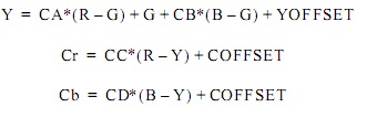
These equations can be directly mapped to the architecture shown in Figure 2. The blue boxes in Figure 3 represent logic blocks, which are always implemented using XtremeDSP slices. [3] Example of time diagram of the conversion is shown in Figure 4.
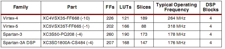
ResultsThe studies used chip Spartan‐3 with a frequency of 178 MHz (Table 1). The result is a performance of 4.4 ms for processing a frame size of 1024x768 pixels. For comparison, treatment of the same image in the Matlab takes 373 ms, significantly higher than at run time on the hardware platform.
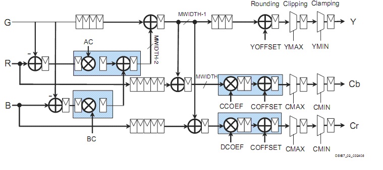
Figure 3: Application Schematic
Figure 4 — Time diagram of the conversion
Table 1 — Table of productivity
The advantages of using this hardware is obvious: speed, ease of replacement of hardware blocks and improve the algorithm itself.
Overview of the JPEG compression algorithmConverting an image from RGB color space to YCbCr (YUV). It should be noted that the standard JPEG (ISO / IEC 10918‐1) can not regulate the choice of YCbCr, allowing other types of transformations (eg, the number of components , different from three) and contraction without conversion (directly in RGB) , but the specification JFIF (JPEG File Interchange Format, proposed in 1991 by specialists of C‐Cube Microsystems, and has become the current de facto standard) propose to use transformation RGB-> YCbCr.[2]
After converting the RGB-> YCbCr images for channels Cb and Cr, that responsible for color, can be done "decimation" (subsampling [3]), which lies in the fact that each block of 4 pixels (2x2) Luminance channel Y placed in correspondence with the average values of Cb and Cr (thinning scheme "4:2:0" [4]). Moreover, for each block of 2x2 instead of 12 values (4 Y, Cb and 4 4 Cr) is used only 6 (4 Y, and one averaged Cb and Cr). If the quality of the reconstructed images after compression must increase, the decimation can be performed only in some one direction — vertically (scheme "4:4:0") or horizontally (the 4:2:2 "), or not performed altogether (4:4:4).
Standard also permits decimation with averaging Cb and Cr not for the 2x2 block, but for four pixels located sequentially (vertically or horizontally), ie, for blocks of 1x4 or a 4x1 (scheme "4:1:1"). It is also possible to use different types of decimation for Cb and Cr, but in practice such schemes are found rarely.
Furthermore, luminance Y and responsible for color components Cb and Cr are broken down into 8x8 blocks of pixels. Each unit undergoes a Discrete Cosine Transform (DCT). These DCT coefficients are quantizing (for Y, Cb and Cr, in general, use different quantization matrix) and packed using Huffman codes. JPEG standard also allows the use of much more efficient arithmetic coding, however, due to patent restrictions (described in the patent for the standard JPEG arithmetic QM‐coder belongs to IBM), in practice it is not used.
The high compression efficiency, which gives this algorithm is based on the fact that in the matrix of frequency coefficients generated from the original matrix after the discrete cosine transform, low‐frequency components are located closer to the top left corner, while the high‐frequency — the bottom right corner. This is important because most graphic images on a computer screen is composed of low frequency information, so high‐frequency components of the matrix can be safely discarded. Throwing done by rounding frequency coefficients. After rounding the nonzero value of low‐frequency components remain in the upper left corner of the matrix. Rounded values of the matrix is encoded in the light of repetitions of zeros. As a result, the graphic image is compressed more than 90%, losing very little in quality of image only at the stage of rounding.
Practical value
FPGA architecture is more flexible, at its base can be implemented parallelization of operations, which increases the productivity of all DSP‐system. Common examples of such use FPGA — Implementation of FIR filters, fast Fourier transform, the digital transformation with decreasing frequency, block FEC [7].
Technology based on FPGA allows to solve a real‐time problem detection and recognition, as well as their characteristics (eg, linear dimensions, speed, coordinates, etc.). [8]
Areas of work:
- imaging with the IR receivers
- image processing
- pattern recognition
Sources of images:
- infrared or video camera
- stereo vision
- multispectral image
Classes tasks:
- object on a separate image (including multispectral stereo)
- movable object on a sequence of images obtained stationary receiver
- stationary object on a sequence of images from a stationary receiver
- movable object on a sequence of images acquired mobile receiver
- stationary object on a sequence of images from a mobile receiver
A review of research on the topic in DonNTU
Mukha Yevgen Mihaylovych
Theme of master's work:
«Research implementations MPEG2 video processors on the FPGA and PRUS»
http://masters.donntu.ru/2005/fvti/mukha/diss/index.htm
Gennadiy Voitov
Theme of master's work:
«Digital signal processing in FPGA»
http://masters.donntu.ru/2009/fvti/voitovg/diss/index.htm
DRUZHYNIN OLEKSIY
Theme of master's work:
«DEVELOPMENT OF MULTIPLE‐PROCESSOR SYSTEMS TO SOLVE DIFFERENTIAL EQUATIONS
ON THE BASIS OF FPGA»
http://masters.donntu.ru/2006/fvti/druzhynin/diss/index.htm
Similyetov Alexandr Sergeevich
Theme of master's work:
«Research of structures of 3d accelerators, which uses FPGA technologies»
http://masters.donntu.ru/2004/fvti/similyetov/diss/index.htm
Sergey N. Svistunov
Theme of master's work:
«Research and development on FPGA SPP‐architecture of the control post of digital devices»
http://masters.donntu.ru/2008/fvti/svistunov/diss/index.html
Vladimir O. Kuz'menko
Theme of master's work:
«Automation of designing high‐speed digital devices on FPGA»
http://masters.donntu.ru/2008/fvti/kuzmenko/diss/index.htm
Vypritskaya Polina Alexandrovna
Theme of master's work:
«Automatisation of Mealy automaton synthesis on FPGA»
http://masters.donntu.ru/2008/fvti/vypritskaya/diss/index.htm
Gez Michael Valerievich
Theme of master's work:
«Simulation of HDL‐projects on a multiprocessor system»
http://masters.donntu.ru/2003/fvti/gez/diss/index.htm
From this list of Master works we can be conclude that the FPGA has long been a topical area for research in different fields and still represents an interest.
A review of research on the topic in Ukraine and the world
Since 1984, when the world first released the Xilinx programmable logic (FPGA) architecture with FPGA (Field Programmable Gate Array), and the company is currently the world's leading manufacturer of programmable logic chips. Technology Xilinx provide an opportunity for hardware manufacturers to minimize the risks by reducing the time to develop new products and the timing of its entry. Developers can design and do debugging their unique devices based on Xilinx FPGA is much faster than using traditional methods, in which chips are a fixed structure, at the time of their manufacture. Moreover, because Xilinx FPGAs are ready to programming standard products, the developers do not need to wait for prototypes or to make substantial expenditures for the pre‐production, as when using the fixed‐logic or ASIC (Applications Specific Integrated Circuit). Currently, Xilinx products are widely used — from telecommunications and consumer electronics to the automobile and industrial equipment.
The essence of the market FPGAThere are two important trends in the development of semiconductor industry: the evolution of the technological process of chip, which allows to continue to follow Moore's law and reduce the cost of products, as well as increasing productivity and reducing cost programmable chips, which allows to reach an unprecedented level of customization and flexibility at very affordable prices. Following this trend, Xilinx works in various segments of the market of electronic equipment and makes its products suitable for a wider range of applications.
Manufacturers of devices for handling data, consumer electronics, communication devices, industrial automation, measurement systems, devices, defense and aerospace industry using Xilinx FPGAs as the foundation of their projects.
In Ukraine, the Institute of Cybernetics. VI Glushkov in the Department of microprocessor technology compiled a large list of publications on the FPGA.
http://www.incyb.kiev.ua/s/284/ua/biblioteka_osnownyh_publikatsiy_/_otdel_mikroprotsessor.html
Conclusion
It can be noted that the development of architecture and the FPGA element base has recently significant impact not only on the practical side of designing digital processing systems, but also allowed the hardware implementation of these algorithms, which previously had no practical significance because of the extremely low productivity of the use of standard computational tools. However, the emergence of new families, including the introduction of the properties of high performance FPGA devices in a low cost, allows a wide range of developers to use in their projects the power of modern methods of digital signal processing, including algorithms, focused on parallel computing. Good software support and high demand for digital systems makes products based on FPGA effective and competitive.
Literature
- Кузелин М.О. , Кнышев Д.А., Зотов В.Ю. Современные семейства ПЛИС фирмы Xilinx: справочное пособие. – 440 с.
- Тарасов И.Е. Разработка цифровых устройств на основе ПЛИС Xilinx с применением языка VHDL – 252 c.
- RGB to YCrCb Color‐Space Converter v1.0 DS659 March 24, 2008 Product Specification – 6 с., 15 с., 17 с.
- Гонсалес Р., Цифровая обработка изображений в среде MATLAB – 206 с., 216 с.
- Тематический журнал «Компоненты и технологии». [Электронный ресурс]/ — Электронные данные — Режим доступа: http://www.kit-e.ru/index.php, свободный
- Журнал «Электронные компоненты», 1999, №5. [Электронный ресурс]/ — Электронные данные — Режим доступа: http://www.elcp.ru/index.php?state=izd&i_izd=elcomp&i_num=1999_05&i_art=12, свободный
- «ЭЛЕКТРОНИКА: Наука, Технология, Бизнес» российский научно‐технический журнал, освещающий проблемы электроники в её широком понимании. [Электронный ресурс]/ — Электронные данные — Режим доступа: http://www.electronics.ru/, свободный
- Официальный сайт НТЦ "Модуль" — лидирующая российская hi‐tech‐компания, работающая в области электроники. [Электронный ресурс]/ — Электронные данные — Режим доступа: http://www.module.ru, свободный
Note.
In writing this essay master's work is not yet completed. Final completion: December 2010. Full text of work and materials on the subject can be obtained from the author or his manager after that date.