Тематическая статья №1
1. DESIGN SECURITY WITH WAVEFORMS
Авторы:
Jie Feng, Joel A. Seely, Altera Corporation
Описание: Защита авторских прав на IP ядра, погружаемые на ПЛИСы стоит очень остро. Надежный способ - шифрование. В статье ведется разговор о принципах шифрования IP ядер и работе зашифрованных ядер, погруженных на ПЛИС.
Источник:
http://www.altera.com/literature/cp/cp_sdr_design_security.pdf
DESIGN SECURITY WITH WAVEFORMS
Jie Feng
Altera Corporation
101 Innovation Dr
San Jose, CA 95134
(408) 544-6753
jfeng@altera.com
Joel A. Seely
Altera Corporation
101 Innovation Dr
San Jose, CA 95134
(408) 544-8122
jseely@altera.com
ABSTRACT
Military communications applications such as the Joint tactical Radio System (JTRS) are increasingly turning to FPGAs for large portions of their system design. The reasons for this are many, but include the benefits of increased density, functionality, and performance of FPGAs, as well as higher flexibility, lower development costs and risks over ASICs. However, as FPGAs become a more integral part of the leading edge architectural design, replacing ASICs and ASSPs, security of the FPGA design and configuration bitstream is of utmost importance. This paper describes two techniques – configuration bitstream encryption and handshaking tokens – for securing designers’ intellectual property (IP) within SRAM-based FPGAs.
1. INTRODUCTION
Military applications are becoming increasingly complex. Major programs such as the Future Combat Systems (FCS) and Joint Tactical Radio System (JTRS) are pushing technological capabilities on all fronts to their limits. The electronics in these systems are relying on programmable logic and FPGAs to provide extreme flexibility at a reasonable cost while not giving up the requisite computational power. For example, secure communication systems are used to connect a variety of airborne, space ground and sea-based military communication networks. They are used in the transmission, processing, recording, monitoring and dissemination functions of a variety such networks, including secure data links. All this functionality requires processing power and reconfigurability.
As FPGAs advance in density, functionality and performance, they are increasingly used in critical military system functions that were traditionally filled by ASICs or ASSPs. However, SRAM-based FPGAs are volatile and require a configuration bitstream to be sent from a flash memory or configuration device to the FPGA at power up. Since this bitstream could be intercepted during transmission, design security in high-performance FPGAs is a concern.
2. TECHNIQUES FOR ENSURING BITSTREAM SECURITY
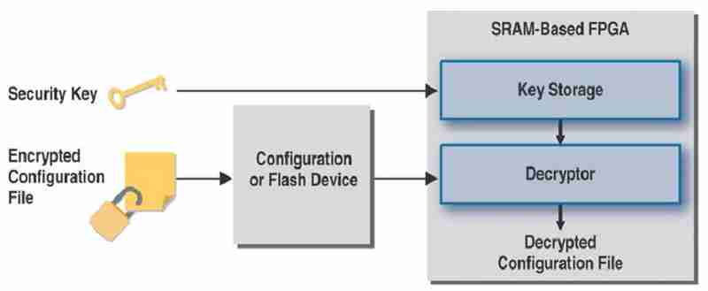
Two techniques – configuration bitstream encryption and handshaking tokens – can be used for securing intellectual property (IP) within SRAM-based FPGAs. The bitstream encryption is enabled using 128-bit advanced encryption standard (AES) and a non-volatile key. The 128-bit AES key makes it much more secure than data encryption standard (DES - 56-bit key size) and triple DES (112-bit effective key size). The non-volatile key is stored on the FPGA and retains its information when power is off, eliminating the need for unreliable battery backup in harsh military environments. Handshaking tokens is a method whereby the FPGA communicates with a CPLD which includes a non-volatile stored encrypted token. The FPGA design must read this token and have the matching key, otherwise the design will shut down.

Figure 1: Altera DSP Builder Design Flow
AES comes in three different key sizes: 128-bit, 192-bit, and 256-bit. The longer the key size, the more secure, but also the more processing-intensive and costly. For many applications, 128-bit AES key size is probably the most suitable for both security and efficiency. To understand the level of security, studies have shown that if one could build a machine that could discover a DES key in seconds, then it would take that same machine approximately 149 trillion years to discover a 128-bit AES key.
Security key storage, which can be in either a volatile or non-volatile location, is an important part of overall security. When the key is stored in volatile memory, an external backup battery is required when there is no power to the device. While this solution is quite secure (because the key will likely be lost if someone tries to attack the solution by decapping the device), reliability, especially in military environments, is a major concern. Battery life depends on temperature and moisture levels of the surrounding area. If the battery dies, the key will be lost, and the device becomes unusable and must be sent back to the factory for repair. Also, adding a battery increases overall system cost and requires additional manufacturing steps. The battery needs to be soldered onto the board after the reflow process. The volatile key needs to be programmed into the FPGA after both the FPGA and the battery are on board.
When the key is stored in a non-volatile location, no external battery is required. This method is more reliable, practical and flexible. The key can be stored into the FPGA during regular manufacturing flow, with the FPGA either on-board or off-board. Various security techniques need to be employed to make the key difficult to find.
Because only the encrypted configuration file is physically located in the system with the key stored securely inside the FPGA, even if the configuration bitstream is captured, it cannot be decrypted. Read-back of a decrypted configuration file is not allowed by the FPGA vendors.
Further, the encrypted configuration file cannot be interpreted and used to configure another FPGA without the appropriate key, making it very difficult to copy such a design.
Reverse engineering any FPGA design through configuration bitstream is very difficult and time- consuming, even without encryption. For high-density devices, the configuration file could contain millions of bits. Some FPGA vendors’ configuration file formats are proprietary and confidential, providing another layer of security. With the addition of configuration bitstream encryption, it may be easier and quicker to build a competitive design from scratch than to reverse engineer such a design.
Tampering cannot be prevented if a volatile key is used because the key is erasable; once the key is erased, the device can be configured with any configuration file. For the non-volatile key solution, the device can be set to only accept configuration files encrypted with the stored key. A configuration failure signals possible tampering with the configuration file, whether in the external memory, during transmission between the external memory and the FPGA, or during remotely communicated system upgrades. This is another advantage of a non-volatile key.
3. HANDSHAKING TOKENS
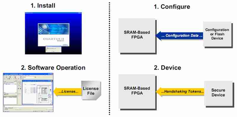
Configuration bitstream encryption is only available in high-density, high-performance SRAM-based FPGAs. The following solution allows any FPGA designs to remain secure even if the configuration bitstream is captured. This is accomplished by disabling the functionality of a user design within the FPGA until handshaking tokens are passed to the FPGA from a secure external device. The secure external device generates continuous handshaking tokens to the FPGA to ensure that it continues operation. This concept is similar to the software license scheme shown in Figure 2.

Figure 2: Comparison of Software License Scheme & FPGA Security Scheme
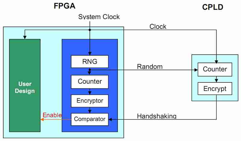
Configuring the FPGA is similar to installing software onto a computer; the configuration bitstream is not protected. The external secure device is similar to the license file. The software will only operate when a valid license file is present. The user design within the FPGA will only operate when the handshaking tokens sent from the external secure device are valid. A simplified hardware implementation for this solution is shown in Figure 3. In this example, a CPLD is used as the secure external device because it is non-volatile and retains its configuration data during power down.

Figure 3: Simplified Hardware Implementation of the FPGA Design Security Solution
After the FPGA is configured, the functionality of the user design within the FPGA is disabled because the enable signal is not asserted, while the security block within the FPGA starts to function. The random number generator (RNG) generates and sends the initial counter value to the CPLD. The CPLD encrypts the counter value and sends the resulting handshaking token to the FPGA. If the handshaking token matches the data generated internally inside the FPGA, the enable signal is asserted, and the user design starts functioning. This process continues during the entire operation of the FPGA. A mismatch will cause the enable signal to go low and disable the functionality of the user design. Figure 4 shows an example of how the enable signal is used with a simple AND gate.

Figure 4: Design with Security Scheme
The FPGA user design only works when the handshaking tokens from the external secure device and the data generated inside the FPGA are identical. Even if the FPGA configuration bitstream is stolen, it is useless, similar to software without a license. Therefore, the FPGA user design is secure from copying. This solution does not provide additional protection against reverse engineering (though difficult) and tampering.
The security of the solution relies on the external secure device to be secure and the handshaking tokens to be unpredictable. A secure external device needs to be non- volatile and retain its configuration during power down (e.g. CPLDs or security processors). The RNG in the solution is critical. It ensures that every time the device starts up, it uses a different initial value. This prevents anyone from storing the handshaking tokens in a storage device. To prevent someone from detecting the pattern in the handshaking tokens, a proven encryption algorithm such as AES should be used.
To ensure that the security scheme works properly, the system clock feeding the FPGA user design should be the same as the system clock feeding the security block. This prevents someone from disabling the security block when the enable signal is asserted. To further increase security, the comparator block can be duplicated several times to produce more enable signals to feed different portions of the user designs.
4. CONCLUSIONS
In an era of ever-increasing security concerns, SRAM-based FPGAs combined with bitstream encryption offer designers of military systems critical advantages. In addition to high density, high performance, low development risk and fast time-to-market benefits over other implementations, they also deliver a secure approach for protecting proprietary designs and IP. For FPGAs without this built-in security feature, an additional non-volatile device can be used to protect the FPGA design by supplying handshaking tokens.
5. REFERENCES
[1] Design Security using MAX II CPLDs, Altera
http://www.altera.com/literature/wp/wp_m2dsgn.pdf
[2] Design Security in Stratix II Devices, Altera
http://www.altera.com/products/devices/stratix2/features/security/st2-security.html